参数资料
| 型号: | A54SX16P-1TQ144 |
| 厂商: | Microsemi SoC |
| 文件页数: | 56/64页 |
| 文件大小: | 0K |
| 描述: | IC FPGA SX 24K GATES 144-TQFP |
| 标准包装: | 60 |
| 系列: | SX |
| LAB/CLB数: | 1452 |
| 输入/输出数: | 113 |
| 门数: | 24000 |
| 电源电压: | 3 V ~ 3.6 V,4.75 V ~ 5.25 V |
| 安装类型: | 表面贴装 |
| 工作温度: | 0°C ~ 70°C |
| 封装/外壳: | 144-LQFP |
| 供应商设备封装: | 144-TQFP(20x20) |
第1页第2页第3页第4页第5页第6页第7页第8页第9页第10页第11页第12页第13页第14页第15页第16页第17页第18页第19页第20页第21页第22页第23页第24页第25页第26页第27页第28页第29页第30页第31页第32页第33页第34页第35页第36页第37页第38页第39页第40页第41页第42页第43页第44页第45页第46页第47页第48页第49页第50页第51页第52页第53页第54页第55页当前第56页第57页第58页第59页第60页第61页第62页第63页第64页
SX Family FPGAs
1- 2
v3.2
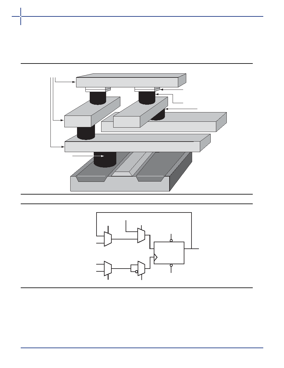
The R-cell contains a flip-flop featuring asynchronous
clear, asynchronous preset, and clock enable (using the
S0 and S1 lines) control signals (Figure 1-2). The R-cell
registers feature programmable clock polarity selectable
on a register-by-register basis. This provides additional
flexibility
while
allowing
mapping
of
synthesized
functions into the SX FPGA. The clock source for the
R-cell can be chosen from either the hardwired clock or
the routed clock.
The C-cell implements a range of combinatorial functions
up to 5-inputs (Figure 1-3 on page 1-3). Inclusion of the
DB input and its associated inverter function dramatically
increases the number of combinatorial functions that can
be implemented in a single module from 800 options in
previous architectures to more than 4,000 in the SX
architecture. An example of the improved flexibility
enabled by the inversion capability is the ability to
integrate a 3-input exclusive-OR function into a single
C-cell. This facilitates construction of 9-bit parity-tree
functions with 2 ns propagation delays. At the same
time, the C-cell structure is extremely synthesis friendly,
simplifying the overall design and reducing synthesis
time.
Figure 1-1
SX Family Interconnect Elements
Figure 1-2
R-Cell
Silicon Substrate
Tungsten Plug
Contact
Metal 1
Metal 2
Metal 3
Routing Tracks
Amorphous Silicon/
Dielectric Antifuse
Tungsten Plug Via
Direct
Connect
Input
CLKA, CLKB,
Internal Logic
HCLK
CKS
CKP
CLRB
PSETB
Y
DQ
Routed Data Input
S0
S1
相关PDF资料 |
PDF描述 |
|---|---|
| A1010B-2VQ80C | IC FPGA 1200 GATES 80-VQFP COM |
| A1010B-2VQG80C | IC FPGA 1200 GATES 80-VQFP COM |
| M7A3P1000-1FG144I | IC FPGA 1KB FLASH 1M 144-FBGA |
| M7A3P1000-1FGG144I | IC FPGA 1KB FLASH 1M 144-FBGA |
| A42MX09-3TQ176I | IC FPGA MX SGL CHIP 14K 176-TQFP |
相关代理商/技术参数 |
参数描述 |
|---|---|
| A54SX16P-1TQ144I | 功能描述:IC FPGA SX 24K GATES 144-TQFP RoHS:否 类别:集成电路 (IC) >> 嵌入式 - FPGA(现场可编程门阵列) 系列:SX 产品培训模块:Three Reasons to Use FPGA's in Industrial Designs Cyclone IV FPGA Family Overview 特色产品:Cyclone? IV FPGAs 标准包装:60 系列:CYCLONE® IV GX LAB/CLB数:9360 逻辑元件/单元数:149760 RAM 位总计:6635520 输入/输出数:270 门数:- 电源电压:1.16 V ~ 1.24 V 安装类型:表面贴装 工作温度:0°C ~ 85°C 封装/外壳:484-BGA 供应商设备封装:484-FBGA(23x23) |
| A54SX16P-1TQ144M | 功能描述:IC FPGA SX 24K GATES 144-TQFP RoHS:否 类别:集成电路 (IC) >> 嵌入式 - FPGA(现场可编程门阵列) 系列:SX 标准包装:1 系列:ProASICPLUS LAB/CLB数:- 逻辑元件/单元数:- RAM 位总计:129024 输入/输出数:248 门数:600000 电源电压:2.3 V ~ 2.7 V 安装类型:表面贴装 工作温度:- 封装/外壳:352-BFCQFP,带拉杆 供应商设备封装:352-CQFP(75x75) |
| A54SX16P-1TQ176 | 功能描述:IC FPGA SX 24K GATES 176-TQFP RoHS:否 类别:集成电路 (IC) >> 嵌入式 - FPGA(现场可编程门阵列) 系列:SX 标准包装:40 系列:SX-A LAB/CLB数:6036 逻辑元件/单元数:- RAM 位总计:- 输入/输出数:360 门数:108000 电源电压:2.25 V ~ 5.25 V 安装类型:表面贴装 工作温度:0°C ~ 70°C 封装/外壳:484-BGA 供应商设备封装:484-FPBGA(27X27) |
| A54SX16P-1TQ176I | 功能描述:IC FPGA SX 24K GATES 176-TQFP RoHS:否 类别:集成电路 (IC) >> 嵌入式 - FPGA(现场可编程门阵列) 系列:SX 产品培训模块:Three Reasons to Use FPGA's in Industrial Designs Cyclone IV FPGA Family Overview 特色产品:Cyclone? IV FPGAs 标准包装:60 系列:CYCLONE® IV GX LAB/CLB数:9360 逻辑元件/单元数:149760 RAM 位总计:6635520 输入/输出数:270 门数:- 电源电压:1.16 V ~ 1.24 V 安装类型:表面贴装 工作温度:0°C ~ 85°C 封装/外壳:484-BGA 供应商设备封装:484-FBGA(23x23) |
| A54SX16P-1TQG144 | 功能描述:IC FPGA SX 24K GATES 144-TQFP RoHS:是 类别:集成电路 (IC) >> 嵌入式 - FPGA(现场可编程门阵列) 系列:SX 标准包装:40 系列:SX-A LAB/CLB数:6036 逻辑元件/单元数:- RAM 位总计:- 输入/输出数:360 门数:108000 电源电压:2.25 V ~ 5.25 V 安装类型:表面贴装 工作温度:0°C ~ 70°C 封装/外壳:484-BGA 供应商设备封装:484-FPBGA(27X27) |
发布紧急采购,3分钟左右您将得到回复。