- 您现在的位置:买卖IC网 > PDF目录19336 > A54SX32A-TQG100 (Microsemi SoC)IC FPGA 249I/O 100TQFP PDF资料下载
参数资料
| 型号: | A54SX32A-TQG100 |
| 厂商: | Microsemi SoC |
| 文件页数: | 12/108页 |
| 文件大小: | 0K |
| 描述: | IC FPGA 249I/O 100TQFP |
| 标准包装: | 90 |
| 系列: | SX-A |
| LAB/CLB数: | 2880 |
| 输入/输出数: | 81 |
| 门数: | 48000 |
| 电源电压: | 2.25 V ~ 5.25 V |
| 安装类型: | 表面贴装 |
| 工作温度: | 0°C ~ 70°C |
| 封装/外壳: | 100-LQFP |
| 供应商设备封装: | 100-TQFP(14x14) |
| 其它名称: | 1100-1072 |
第1页第2页第3页第4页第5页第6页第7页第8页第9页第10页第11页当前第12页第13页第14页第15页第16页第17页第18页第19页第20页第21页第22页第23页第24页第25页第26页第27页第28页第29页第30页第31页第32页第33页第34页第35页第36页第37页第38页第39页第40页第41页第42页第43页第44页第45页第46页第47页第48页第49页第50页第51页第52页第53页第54页第55页第56页第57页第58页第59页第60页第61页第62页第63页第64页第65页第66页第67页第68页第69页第70页第71页第72页第73页第74页第75页第76页第77页第78页第79页第80页第81页第82页第83页第84页第85页第86页第87页第88页第89页第90页第91页第92页第93页第94页第95页第96页第97页第98页第99页第100页第101页第102页第103页第104页第105页第106页第107页第108页
SX-A Family FPGAs
v5.3
1-7
Other Architectural Features
Technology
The Actel SX-A family is implemented on a high-voltage,
twin-well CMOS process using 0.22
μ /0.25 μ design
rules. The metal-to-metal antifuse is comprised of a
combination of amorphous silicon and dielectric material
with barrier metals and has a programmed ('on' state)
resistance of 25
Ω with capacitance of 1.0 fF for low
signal impedance.
Performance
The unique architectural features of the SX-A family
enable the devices to operate with internal clock
frequencies of 350 MHz, causing very fast execution of
even complex logic functions. The SX-A family is an
optimal
platform
upon
which
to
integrate
the
functionality previously contained in multiple complex
programmable logic devices (CPLDs). In addition, designs
that previously would have required a gate array to meet
performance goals can be integrated into an SX-A device
with dramatic improvements in cost and time-to-market.
Using timing-driven place-and-route tools, designers can
achieve highly deterministic device performance.
User Security
Reverse engineering is virtually impossible in SX-A
devices because it is extremely difficult to distinguish
between programmed and unprogrammed antifuses. In
addition, since SX-A is a nonvolatile, single-chip solution,
there is no configuration bitstream to intercept at device
power-up.
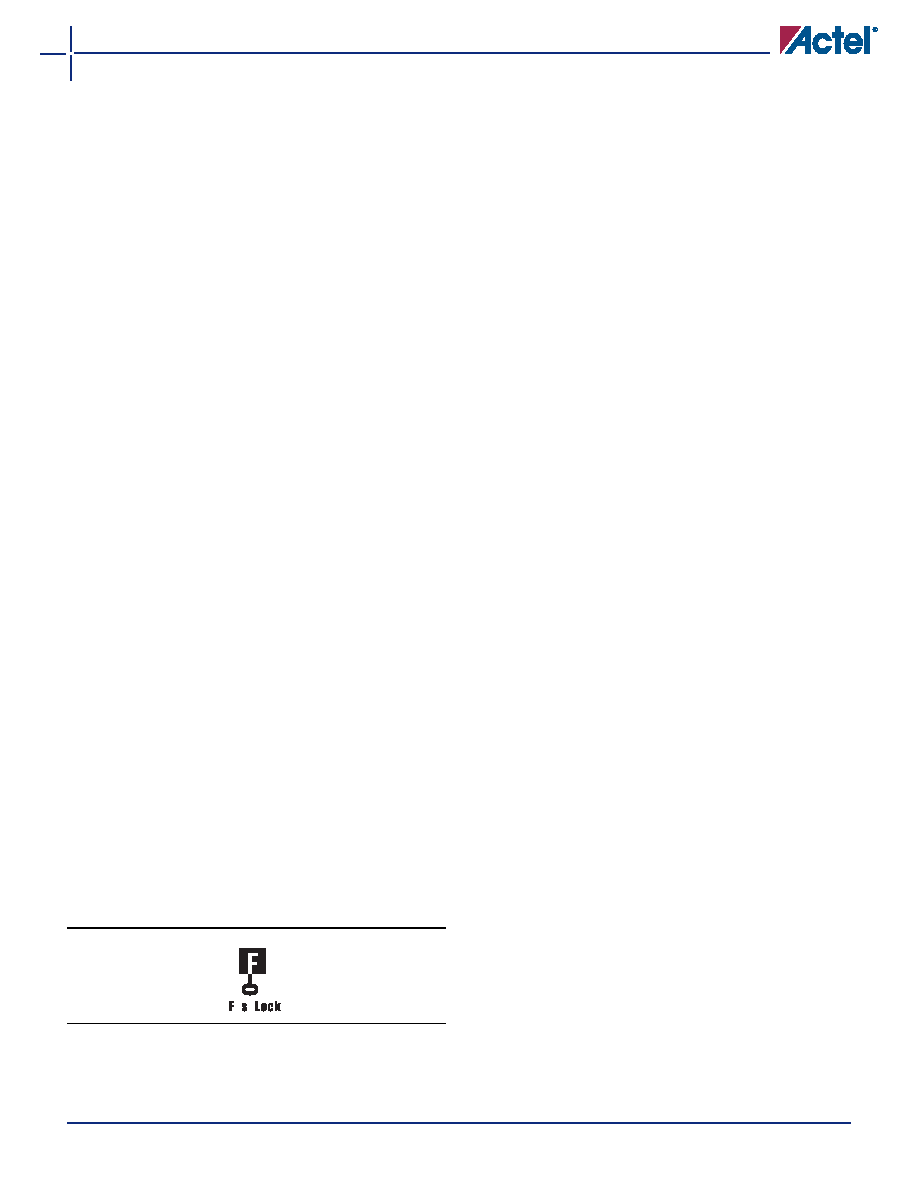
The Actel FuseLock advantage ensures that unauthorized
users will not be able to read back the contents of an
Actel antifuse FPGA. In addition to the inherent
strengths of the architecture, special security fuses that
prevent internal probing and overwriting are hidden
throughout the fabric of the device. They are located
where they cannot be accessed or bypassed without
destroying access to the rest of the device, making both
invasive and more-subtle noninvasive attacks ineffective
against Actel antifuse FPGAs.
Look for this symbol to ensure your valuable IP is secure
For more information, refer to Actel’s Implementation of
Security in Actel Antifuse FPGAs application note.
I/O Modules
For a simplified I/O schematic, refer to Figure 1 in the
application note, Actel eX, SX-A, and RTSX-S I/Os.
Each user I/O on an SX-A device can be configured as an
input, an output, a tristate output, or a bidirectional pin.
Mixed I/O standards can be set for individual pins,
though this is only allowed with the same voltage as the
input. These I/Os, combined with array registers, can
achieve clock-to-output-pad timing as fast as 3.8 ns, even
without the dedicated I/O registers. In most FPGAs, I/O
cells
that
have
embedded
latches
and
flip-flops,
requiring instantiation in HDL code; this is a design
complication not encountered in SX-A FPGAs. Fast pin-
to-pin timing ensures that the device is able to interface
with any other device in the system, which in turn
enables parallel design of system components and
reduces overall design time. All unused I/Os are
configured as tristate outputs by the Actel Designer
software, for maximum flexibility when designing new
boards or migrating existing designs.
SX-A I/Os should be driven by high-speed push-pull
devices with a low-resistance pull-up device when being
configured as tristate output buffers. If the I/O is driven
by a voltage level greater than VCCI and a fast push-pull
device is NOT used, the high-resistance pull-up of the
driver and the internal circuitry of the SX-A I/O may
create a voltage divider. This voltage divider could pull
the input voltage below specification for some devices
connected to the driver. A logic '1' may not be correctly
presented in this case. For example, if an open drain
driver is used with a pull-up resistor to 5 V to provide the
logic '1' input, and VCCI is set to 3.3 V on the SX-A device,
the input signal may be pulled down by the SX-A input.
Each I/O module has an available power-up resistor of
approximately 50 k
Ω that can configure the I/O in a
known state during power-up. For nominal pull-up and
pull-down resistor values, refer to Table 1-4 on page 1-8
of the application note Actel eX, SX-A, and RTSX-S I/Os.
Just slightly before VCCA reaches 2.5 V, the resistors are
disabled, so the I/Os will be controlled by user logic. See
more information concerning available I/O features.
Figure 1-11 FuseLock
e
u
相关PDF资料 |
PDF描述 |
|---|---|
| LQG15HS7N5J02D | INDUCTOR 7.5NH 300MA 0402 |
| VI-2NK-CY-S | CONVERTER MOD DC/DC 40V 50W |
| VE-BN1-EU-S | CONVERTER MOD DC/DC 12V 200W |
| B82422A1223K100 | INDUCTOR 22UH 140MA 1210 10% |
| EPF10K20TC144-4 | IC FLEX 10K FPGA 20K 144-TQFP |
相关代理商/技术参数 |
参数描述 |
|---|---|
| A54SX32A-TQG100A | 功能描述:IC FPGA SX 48K GATES 100-TQFP RoHS:是 类别:集成电路 (IC) >> 嵌入式 - FPGA(现场可编程门阵列) 系列:SX-A 标准包装:40 系列:SX-A LAB/CLB数:6036 逻辑元件/单元数:- RAM 位总计:- 输入/输出数:360 门数:108000 电源电压:2.25 V ~ 5.25 V 安装类型:表面贴装 工作温度:0°C ~ 70°C 封装/外壳:484-BGA 供应商设备封装:484-FPBGA(27X27) |
| A54SX32A-TQG100I | 功能描述:IC FPGA SX 48K GATES 100-TQFP RoHS:是 类别:集成电路 (IC) >> 嵌入式 - FPGA(现场可编程门阵列) 系列:SX-A 标准包装:40 系列:SX-A LAB/CLB数:6036 逻辑元件/单元数:- RAM 位总计:- 输入/输出数:360 门数:108000 电源电压:2.25 V ~ 5.25 V 安装类型:表面贴装 工作温度:0°C ~ 70°C 封装/外壳:484-BGA 供应商设备封装:484-FPBGA(27X27) |
| A54SX32A-TQG100M | 制造商:Microsemi Corporation 功能描述:FPGA SX-A Family 32K Gates 1800 Cells 238MHz 0.25um Technology 2.5V 100-Pin TQFP 制造商:Microsemi Corporation 功能描述:FPGA SX-A 32K GATES 1800 CELLS 238MHZ 0.25UM/0.22UM 2.5V 100 - Trays |
| A54SX32A-TQG144 | 功能描述:IC FPGA 249I/O 144TQFP RoHS:是 类别:集成电路 (IC) >> 嵌入式 - FPGA(现场可编程门阵列) 系列:SX-A 标准包装:60 系列:XP LAB/CLB数:- 逻辑元件/单元数:10000 RAM 位总计:221184 输入/输出数:244 门数:- 电源电压:1.71 V ~ 3.465 V 安装类型:表面贴装 工作温度:0°C ~ 85°C 封装/外壳:388-BBGA 供应商设备封装:388-FPBGA(23x23) 其它名称:220-1241 |
| A54SX32A-TQG144A | 功能描述:IC FPGA SX 48K GATES 144-TQFP RoHS:是 类别:集成电路 (IC) >> 嵌入式 - FPGA(现场可编程门阵列) 系列:SX-A 标准包装:40 系列:SX-A LAB/CLB数:6036 逻辑元件/单元数:- RAM 位总计:- 输入/输出数:360 门数:108000 电源电压:2.25 V ~ 5.25 V 安装类型:表面贴装 工作温度:0°C ~ 70°C 封装/外壳:484-BGA 供应商设备封装:484-FPBGA(27X27) |
发布紧急采购,3分钟左右您将得到回复。