参数资料
| 型号: | A54SX72A-PQ208I |
| 厂商: | Microsemi SoC |
| 文件页数: | 16/108页 |
| 文件大小: | 0K |
| 描述: | IC FPGA SX-A 108K 208-PQFP |
| 标准包装: | 24 |
| 系列: | SX-A |
| LAB/CLB数: | 6036 |
| 输入/输出数: | 171 |
| 门数: | 108000 |
| 电源电压: | 2.25 V ~ 5.25 V |
| 安装类型: | 表面贴装 |
| 工作温度: | -40°C ~ 85°C |
| 封装/外壳: | 208-BFQFP |
| 供应商设备封装: | 208-PQFP(28x28) |
第1页第2页第3页第4页第5页第6页第7页第8页第9页第10页第11页第12页第13页第14页第15页当前第16页第17页第18页第19页第20页第21页第22页第23页第24页第25页第26页第27页第28页第29页第30页第31页第32页第33页第34页第35页第36页第37页第38页第39页第40页第41页第42页第43页第44页第45页第46页第47页第48页第49页第50页第51页第52页第53页第54页第55页第56页第57页第58页第59页第60页第61页第62页第63页第64页第65页第66页第67页第68页第69页第70页第71页第72页第73页第74页第75页第76页第77页第78页第79页第80页第81页第82页第83页第84页第85页第86页第87页第88页第89页第90页第91页第92页第93页第94页第95页第96页第97页第98页第99页第100页第101页第102页第103页第104页第105页第106页第107页第108页
SX-A Family FPGAs
v5.3
1-11
Probing Capabilities
SX-A devices also provide an internal probing capability
that is accessed with the JTAG pins. The Silicon Explorer II
diagnostic hardware is used to control the TDI, TCK, TMS,
and TDO pins to select the desired nets for debugging.
The user assigns the selected internal nets in Actel Silicon
Explorer II software to the PRA/PRB output pins for
observation. Silicon Explorer II automatically places the
device into JTAG mode. However, probing functionality is
only activated when the TRST pin is driven high or left
floating, allowing the internal pull-up resistor to pull
TRST High. If the TRST pin is held Low, the TAP controller
remains in the Test-Logic-Reset state so no probing can
be performed. However, the user must drive the TRST pin
High or allow the internal pull-up resistor to pull TRST
High.
When selecting the Reserve Probe Pin box as shown in
Figure 1-12 on page 1-9, direct the layout tool to reserve
the PRA and PRB pins as dedicated outputs for probing.
This Reserve option is merely a guideline. If the designer
assigns user I/Os to the PRA and PRB pins and selects the
Reserve
Probe
Pin option, Designer Layout will
override the Reserve Probe Pin option and place the
user I/Os on those pins.
To allow probing capabilities, the security fuse must not
be programmed. Programming the security fuse disables
the JTAG and probe circuitry. Table 1-9 summarizes the
possible device configurations for probing once the
device leaves the Test-Logic-Reset JTAG state.
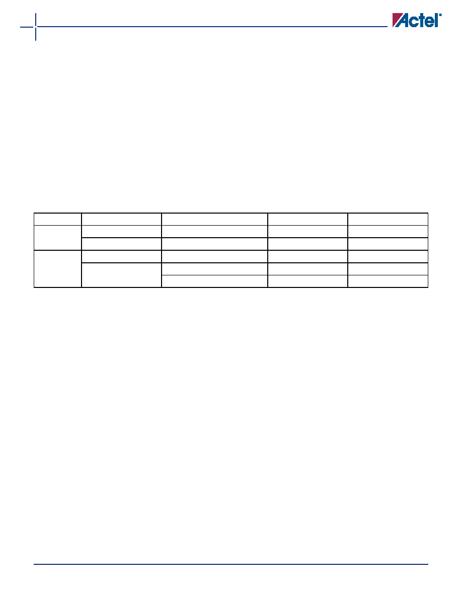
Table 1-9 Device Configuration Options for Probe Capability (TRST Pin Reserved)
JTAG Mode
TRST1
Security Fuse Programmed
PRA, PRB2
TDI, TCK, TDO2
Dedicated
Low
No
User I/O3
JTAG Disabled
High
No
Probe Circuit Outputs
JTAG I/O
Flexible
Low
No
User I/O3
High
No
Probe Circuit Outputs
JTAG I/O
Yes
Probe Circuit Secured
Notes:
1. If the TRST pin is not reserved, the device behaves according to TRST = High as described in the table.
2. Avoid using the TDI, TCK, TDO, PRA, and PRB pins as input or bidirectional ports. Since these pins are active during probing, input
signals will not pass through these pins and may cause contention.
3. If no user signal is assigned to these pins, they will behave as unused I/Os in this mode. Unused pins are automatically tristated by
the Designer software.
相关PDF资料 |
PDF描述 |
|---|---|
| A54SX72A-1PQG208 | IC FPGA SX-A 108K 208-PQFP |
| AMC31DRXN | CONN EDGECARD 62POS .100 DIP SLD |
| AMC31DRXH | CONN EDGECARD 62POS .100 DIP SLD |
| EP1AGX20CF484I6 | IC ARRIA GX FPGA 20K 484FBGA |
| ACC40DRAI | CONN EDGECARD 80POS .100 R/A DIP |
相关代理商/技术参数 |
参数描述 |
|---|---|
| A54SX72A-PQ208IX160 | 制造商:Microsemi Corporation 功能描述:FPGA SX-A 72K GATES 4024 CELLS 217MHZ 0.25UM/0.22UM 2.5V 208 - Trays |
| A54SX72A-PQ208IX3 | 制造商:Microsemi Corporation 功能描述:FPGA SX-A 72K GATES 4024 CELLS 217MHZ 0.25UM/0.22UM 2.5V 208 - Trays |
| A54SX72A-PQ208IX60 | 制造商:Microsemi Corporation 功能描述:FPGA SX-A 72K GATES 4024 CELLS 217MHZ 0.25UM/0.22UM 2.5V 208 - Trays |
| A54SX72A-PQ208M | 制造商:Microsemi Corporation 功能描述:FPGA SX-A Family 72K Gates 4024 Cells 217MHz 0.25um Technology 2.5V 208-Pin PQFP 制造商:Microsemi Corporation 功能描述:FPGA SX-A Family 72K Gates 4024 Cells 217MHz 0.25um/0.22um (CMOS) Technology 2.5V 208-Pin PQFP 制造商:Microsemi Corporation 功能描述:FPGA SX-A 72K GATES 4024 CELLS 217MHZ 0.25UM/0.22UM 2.5V 208 - Trays |
| A54SX72A-PQG208 | 功能描述:IC FPGA 360I/O 208PQFP RoHS:是 类别:集成电路 (IC) >> 嵌入式 - FPGA(现场可编程门阵列) 系列:SX-A 标准包装:60 系列:XP LAB/CLB数:- 逻辑元件/单元数:10000 RAM 位总计:221184 输入/输出数:244 门数:- 电源电压:1.71 V ~ 3.465 V 安装类型:表面贴装 工作温度:0°C ~ 85°C 封装/外壳:388-BBGA 供应商设备封装:388-FPBGA(23x23) 其它名称:220-1241 |
发布紧急采购,3分钟左右您将得到回复。