- 您现在的位置:买卖IC网 > PDF目录364584 > A6812ELW (Allegro MicroSystems, Inc.) DABiC-IV, 20-BIT SERIAL-INPUT, LATCHED SOURCE DRIVER PDF资料下载
参数资料
| 型号: | A6812ELW |
| 厂商: | Allegro MicroSystems, Inc. |
| 元件分类: | 显示驱动器 |
| 英文描述: | DABiC-IV, 20-BIT SERIAL-INPUT, LATCHED SOURCE DRIVER |
| 中文描述: | 达比奇第四,20位串行输入,锁存源驱动 |
| 文件页数: | 5/10页 |
| 文件大小: | 143K |
| 代理商: | A6812ELW |
6812
20-BIT SERIAL-INPUT,
LATCHED SOURCE DRIVER
www.allegromicro.com
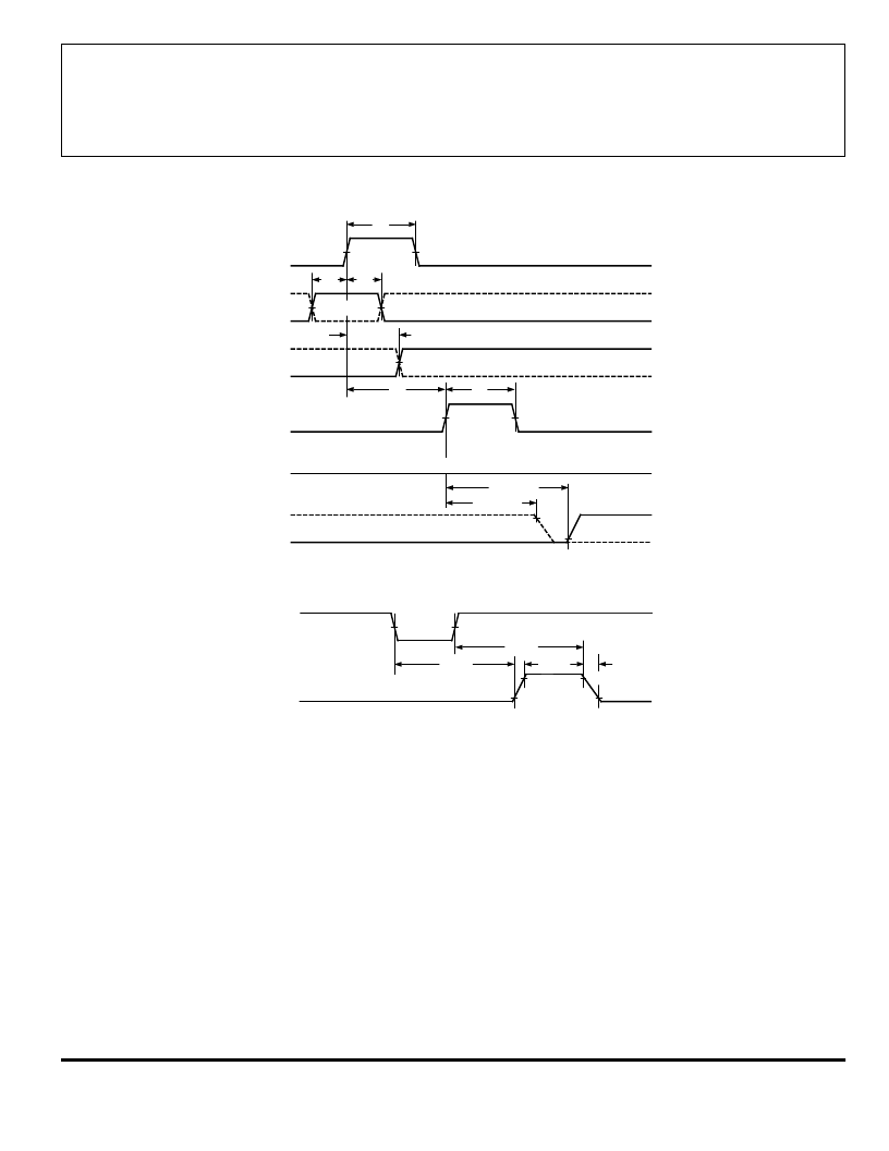
TIMING REQUIREMENTS and SPECIFICATIONS
(Logic Levels are V
DD
and Ground)
Serial Data present at the input is transferred to the shift
register on the logic “0” to logic “1” transition of the CLOCK
input pulse. On succeeding CLOCK pulses, the registers shift
data information towards the SERIAL DATA OUTPUT. The
SERIAL DATA must appear at the input prior to the rising edge
of the CLOCK input waveform.
Information present at any register is transferred to the
respective latch when the STROBE is high (serial-to-parallel
conversion). The latches will continue to accept new data as
long as the STROBE is held high. Applications where the
latches are bypassed (STROBE tied high) will require that the
BLANKING input be high during serial data entry.
When the BLANKING input is high, the output source
drivers are disabled (OFF); the pnp active pull-down sink
drivers are ON. The information stored in the latches is not
affected by the BLANKING input. With the BLANKING input
low, the outputs are controlled by the state of their respective
latches.
CLOCK
SERIAL
DATA IN
STROBE
BLANKING
OUT
N
Dwg. WP-029
50%
SERIAL
DATA OUT
DATA
DATA
10%
90%
50%
50%
50%
C
A
B
D
E
LOW = ALL OUTPUTS ENABLED
p(STH-QL)
t
p(CH-SQX)
t
DATA
p(STH-QH)
t
BLANKING
OUT
N
Dwg. WP-030
DATA
10%
50%
en(BQ)
t
dis(BQ)
t
HIGH = ALL OUTPUTS BLANKED (DISABLED)
90%
r
t
f
t
A.
Data Active Time Before Clock Pulse
(Data Set-Up Time), t
su(D)
......................................
25 ns
B.
Data Active Time After Clock Pulse
(Data Hold Time), t
h(D)
............................................
25 ns
C.
Clock Pulse Width, t
w(CH)
............................................
50 ns
D.
Time Between Clock Activation and Strobe, t
su(C)
....
100 ns
E.
Strobe Pulse Width, t
w(STH)
..........................................
50 ns
NOTE
–
Timing is representative of a 10 MHz clock. Higher
speeds may be attainable with increased supply voltage;
operation at high temperatures will reduce the specified
maximum clock frequency.
相关PDF资料 |
PDF描述 |
|---|---|
| A6812SA | DABiC-IV, 20-BIT SERIAL-INPUT, LATCHED SOURCE DRIVER |
| A6812SEP | DABiC-IV, 20-BIT SERIAL-INPUT, LATCHED SOURCE DRIVER |
| A6812SLW | ECONOLINE: RB & RA - Dual Output from a Single Input Rail- Power Sharing on Output- Industry Standard Pinout- 1kVDC & 2kVDC Isolation- Custom Solutions Available- UL94V-0 Package Material- Efficiency to 85% |
| A6818KA | Vacuum Fluorescent Display Driver |
| A6818KEP | Vacuum Fluorescent Display Driver |
相关代理商/技术参数 |
参数描述 |
|---|---|
| A6812ELW-T | 功能描述:IC SOURCE DRVR 20BIT SER 28-SOIC RoHS:是 类别:集成电路 (IC) >> PMIC - MOSFET,电桥驱动器 - 内部开关 系列:- 标准包装:1,000 系列:- 类型:高端/低端驱动器 输入类型:SPI 输出数:8 导通状态电阻:850 毫欧,1.6 欧姆 电流 - 输出 / 通道:205mA,410mA 电流 - 峰值输出:500mA,1A 电源电压:9 V ~ 16 V 工作温度:-40°C ~ 150°C 安装类型:表面贴装 封装/外壳:20-SOIC(0.295",7.50mm 宽) 供应商设备封装:PG-DSO-20-45 包装:带卷 (TR) |
| A6812ELWTR | 功能描述:IC SOURCE DRVR 20BIT SER 28SOIC RoHS:否 类别:集成电路 (IC) >> PMIC - MOSFET,电桥驱动器 - 内部开关 系列:- 标准包装:1,000 系列:- 类型:高端/低端驱动器 输入类型:SPI 输出数:8 导通状态电阻:850 毫欧,1.6 欧姆 电流 - 输出 / 通道:205mA,410mA 电流 - 峰值输出:500mA,1A 电源电压:9 V ~ 16 V 工作温度:-40°C ~ 150°C 安装类型:表面贴装 封装/外壳:20-SOIC(0.295",7.50mm 宽) 供应商设备封装:PG-DSO-20-45 包装:带卷 (TR) |
| A6812ELWTR-T | 功能描述:IC SOURCE DRVR 20BIT SER 28SOIC RoHS:是 类别:集成电路 (IC) >> PMIC - MOSFET,电桥驱动器 - 内部开关 系列:- 标准包装:1,000 系列:- 类型:高端/低端驱动器 输入类型:SPI 输出数:8 导通状态电阻:850 毫欧,1.6 欧姆 电流 - 输出 / 通道:205mA,410mA 电流 - 峰值输出:500mA,1A 电源电压:9 V ~ 16 V 工作温度:-40°C ~ 150°C 安装类型:表面贴装 封装/外壳:20-SOIC(0.295",7.50mm 宽) 供应商设备封装:PG-DSO-20-45 包装:带卷 (TR) |
| A6812KA | 制造商:未知厂家 制造商全称:未知厂家 功能描述:VACUUM FLUORESCENT DISPLAY DRIVER|BICMOS|DIP|28PIN|PLASTIC |
| A6812KEP | 制造商:未知厂家 制造商全称:未知厂家 功能描述:VACUUM FLUORESCENT DISPLAY DRIVER|BICMOS|LDCC|28PIN|PLASTIC |
发布紧急采购,3分钟左右您将得到回复。