- 您现在的位置:买卖IC网 > PDF目录364590 > AB-075 AB-075 - PHOTODIODE MONITORING WITH OP AMPS PDF资料下载
参数资料
| 型号: | AB-075 |
| 英文描述: | AB-075 - PHOTODIODE MONITORING WITH OP AMPS |
| 中文描述: | 抗体- 075 -光电二极管监测与运算放大器 |
| 文件页数: | 1/2页 |
| 文件大小: | 57K |
| 代理商: | AB-075 |
The CMOS ADS574 and ADS774 are drop-in replacements
for industry standard ADC574 analog-to-digital converters,
offering lower power and the capability to operate from a
single +5V supply. The switched capacitor array architec-
ture (CDAC), with the input resistor divider network to
provide ADC574 input ranges, also allow the new parts to
handle additional input ranges, including a 0V to 5V range.
This can be used to build a complete temperature data
acquisition system using a single +5V supply.
Figure 1 shows the input resistor divider network on the
ADS574, and how it can be configured for a 0V to 5V input
range. Pin 12 is normally the bipolar offset pin on standard
ADC574s, and serves the same function for
±
5V and
±
10V
input ranges on the ADS574. However, when connected as
shown, pin 12 on the ADS574 can also be used as an analog
input. In this mode, the ADS574 can also be used as an
analog input. In this mode, the ADS574 maintains its differ-
ential linearity of 12-bit “No-Missing-Codes”, and integral
linearity is typically better than 0.1%, or 10-bits. The slight
change in linearity is due to internal circuitry designed to
maximize compatibility of the ADS574 used in existing
ADC574 sockets.
Figure 2 shows the circuit for a complete high accuracy
temperature measurement system using the 0V to 5V input
range on the ADS574. The RTD sensor shown has a resis-
tance of 100
at 0
°
C, and is rated for use from –200
°
C to
660
°
C. Over this range, the resistance of the RTD will vary
from about 18
to about 333
.
Amplifiers A
and A
(the two op amps inside a single
OPA1013) are used to generate a stable 1mA current source
to excite the RTD. The 2.5V reference output of the ADS574
is used to derive this current source, so that the entire system
will be ratiometric. As the reference in the ADS574 changes
over temperature or time, it will affect both the gain of the
A/D and the current source.
RTDs in industrial process controls are often far removed
from the electronics. One thousand feet of 22-gauge copper
has 16
of resistance (shown as R
W
in Figure 2), and this
varies with temperature. The circuit around A
3
(half of a
second OPA1013) uses a third wire from the remote RTD to
remove most of the effect of the two R
W
drops in series with
the RTD. The 100k
resistors are much larger than R
W
,
minimizing inaccuracies due to currents flowing through
them.
Amplifier A
is used in a gain of 12.207V/V, so that a 0.1
change in the value of the RTD (changing the positive input
to A
by 100
μ
V) corresponds to one LSB change in the
output of the ADS574. 0V and 5V full scale inputs to the
ADS574 would result from 0
and 409.6
RTD values
(and hence 0mV and 409.6mV at A
’s input.) Choosing this
range not only sets one LSB equal to a 0.1
change, but also
keeps A
and A
from ever operating near their 0V and 5V
rails. The RTD never gets below about 18
or above about
330
, which gives 18mV to 330mV at the input to A
(and
somewhat more at the input to A
3
, due to the two R
W
drops.)
As used in Figure 2, the ADS574 will switch to the hold
mode and start a conversion immediately when a convert
command is received (a falling edge on pin 5.) Pin 28 will
output a HIGH during conversion, and a falling edge output
on pin 28 can be used to read the data from the conversion.
Since digital processing will normally be done to linearize
the output of the RTD for maximum accuracy, the same
process can also be used to calibrate out gain and offset
errors in the circuit, and any effects from the approximations
used in the feedback around A
3
.
This linearization will also restore the integral linearity of
the ADS574 mentioned above, since the differential linear-
ity remains at the 12-bit level.
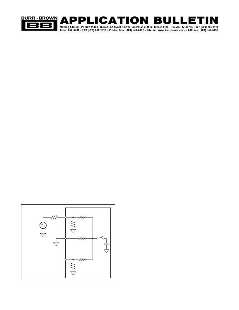
FIGURE 1. ADS574 Connections for 0V to +5V Input
Range.
ADS574
17k
68k
34k
34k
10k
12
0V to +5V
Input Signal
20pF
50
14
No
Connection
13
0V to
3.33V
1994 Burr-Brown Corporation
AB-070
Printed in U.S.A. January, 1994
COMPLETE TEMPERATURE DATA
ACQUISITION SYSTEM FROM A SINGLE +5V SUPPLY
by George Hill, (602) 746-7283
相关PDF资料 |
PDF描述 |
|---|---|
| AB-076 | AB-076 - Noise Analysis of FET Transimpedance Amplifiers |
| AB-087 | AB-087 - LEVEL SHIFTING SIGNALS WITH DIFFERENTIAL AMPLIFIERS |
| AB-088 | AB-088 - IMPROVED VOLTAGE REFERENCE FILTER HAS SEVERAL ADVANTAGES |
| AB-089 | AB-089 - A CLARIFICATION OF USE HIGH-SPEED S/H TO IMPROVE SAMPLING ADC PERFORMANCE |
| AB-090 | AB-090 - FEEDBACK CIRCUIT CLAMPS PRECISELY |
相关代理商/技术参数 |
参数描述 |
|---|---|
| AB-0751BA-01WA-P30-S | 制造商:A-BRIGHT 制造商全称:A-BRIGHT Inc 功能描述:HIGH POWER LED BULB |
| AB-0751GA-01WA-P30-S | 制造商:A-BRIGHT 制造商全称:A-BRIGHT Inc 功能描述:HIGH POWER LED BULB |
| AB-0751RA-01WA-P30-S | 制造商:A-BRIGHT 制造商全称:A-BRIGHT Inc 功能描述:HIGH POWER LED BULB |
| AB-0751SW-01WA-P30-S | 制造商:A-BRIGHT 制造商全称:A-BRIGHT Inc 功能描述:HIGH POWER LED BULB |
| AB-076 | 制造商:未知厂家 制造商全称:未知厂家 功能描述:AB-076 - Noise Analysis of FET Transimpedance Amplifiers |
发布紧急采购,3分钟左右您将得到回复。