- 您现在的位置:买卖IC网 > PDF目录223306 > ACPL-K342-000E 1 CHANNEL LOGIC OUTPUT OPTOCOUPLER PDF资料下载
参数资料
| 型号: | ACPL-K342-000E |
| 元件分类: | 光电耦合器 |
| 英文描述: | 1 CHANNEL LOGIC OUTPUT OPTOCOUPLER |
| 封装: | ROHS COMPLIANT, PLASTIC, SOP-8 |
| 文件页数: | 7/19页 |
| 文件大小: | 333K |
| 代理商: | ACPL-K342-000E |
15
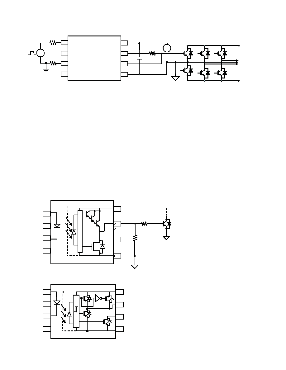
Figure 33. Recommended application circuit with split resistors LED drive and active Miller Clamp.
+
_
1
2
3
4
8
7
6
5
VCC
VOUT
VCLAMP
VEE
CATHODE
NC
ANODE
+
_
RG
Q1
Q2
+
VCE
-
R
+ HVDC
-HVDC
3-PHASE
AC
+
VCE
-
1
PF
R
NC
VCC=18V
+
_
+
_
+
Active Miller Clamp
A Miller clamp allows the control of the Miller current
during a high dV/dt situation. And it can also eliminate
the use of a negative supply voltage by quickly discharg-
ing the large gate capacitance of IGBT to low level without
affecting the IGBT turn-off characteristics. During turn-off,
the gate voltage is monitored and the clamp output is
activated when gate voltage goes below 2.3V (relative to
VEE). The clamp voltage is VOL+2.5V typ for a Miller current
up to 2.5 A. The clamp is disabled when the LED input is
triggered again.
AN5314 application note describes how the clamp reduces
the parasitic turn-on effect due to the Miller capacitor and
at the same time eliminates the need of a negative power
supply.
The Miller pin should be connected to VEE when not in use.
Rail-to-Rail Output
Figure 34 shows a typical gate driver’s high current
output stage with 3 bipolar transistors in darlington con-
figuration. During the output high transition, the output
voltage rises rapidly to within 3 diode drops of VCC. To
ensure the VOUT is at VCC in order to achieve IGBT rated
VCE(ON) voltage. The level of VCC will be need to be raised
to beyond VCC+3(VBE) to account for the diode drops. And
to limit the output voltage to VCC, a pull-down resistor,
RPULL-DOWN between the output and VEE is recommended
to sink a static current while the output is high.
ACPL-H342 uses a power NMOS follower stage to deliver
the initial large current and a smaller PMOS to pull it to VCC
to achieve Rail-to-Rail output voltage as shown in Figure
35. This ensures that the IGBT’s gate voltage is driven to
the optimum intended level with no power loss across
IGBT even when an unstable power supply is used.
Figure 34. Typical gate driver with output stage in darlington configuration
Figure 35. ACPL-H342 with NMOS and PMOS output stage for Rail-to-Rail output voltage
1
2
3
4
8
7
6
5
VCC
VOUT
VEE
CATHODE
NC
ANODE
NC
RG
RPULL-DOWN
VCC
VOUT
VCLAMP
VEE
1
2
3
4
8
7
6
5
CATHODE
NC
ANODE
NC
相关PDF资料 |
PDF描述 |
|---|---|
| ACPL-P454-500 | 1 CHANNEL LOGIC OUTPUT OPTOCOUPLER |
| ACR7HYA58CFREQ | TCXO, CLOCK, 0.5 MHz - 160 MHz, ACMOS OUTPUT |
| ACS7HXCB7CFREQ | TCXO, CLOCK, 0.5 MHz - 160 MHz, ACMOS OUTPUT |
| ACS5HXB17CFREQ | TCXO, CLOCK, 0.5 MHz - 160 MHz, ACMOS OUTPUT |
| ACR5HYB17CFREQ | TCVCXO, CLOCK, 0.5 MHz - 160 MHz, ACMOS OUTPUT |
相关代理商/技术参数 |
参数描述 |
|---|---|
| ACPL-K342-060E | 功能描述:逻辑输出光电耦合器 Optocoupler RoHS:否 制造商:Fairchild Semiconductor 绝缘电压:4243 Vrms 输出类型:Push-Pull 最大传播延迟时间:500 ns 最大正向二极管电压: 最大反向二极管电压: 最大正向二极管电流: 最大连续输出电流:2.5 A 最大功率耗散:100 mW 最大工作温度:+ 100 C 最小工作温度:- 40 C 封装 / 箱体:SO-16 封装:Tube |
| ACPL-K342-500E | 功能描述:逻辑输出光电耦合器 Optocoupler RoHS:否 制造商:Fairchild Semiconductor 绝缘电压:4243 Vrms 输出类型:Push-Pull 最大传播延迟时间:500 ns 最大正向二极管电压: 最大反向二极管电压: 最大正向二极管电流: 最大连续输出电流:2.5 A 最大功率耗散:100 mW 最大工作温度:+ 100 C 最小工作温度:- 40 C 封装 / 箱体:SO-16 封装:Tube |
| ACPL-K342-560E | 功能描述:逻辑输出光电耦合器 Optocoupler RoHS:否 制造商:Fairchild Semiconductor 绝缘电压:4243 Vrms 输出类型:Push-Pull 最大传播延迟时间:500 ns 最大正向二极管电压: 最大反向二极管电压: 最大正向二极管电流: 最大连续输出电流:2.5 A 最大功率耗散:100 mW 最大工作温度:+ 100 C 最小工作温度:- 40 C 封装 / 箱体:SO-16 封装:Tube |
| ACPL-K34T | 制造商:AVAGO 制造商全称:AVAGO TECHNOLOGIES LIMITED 功能描述:Automotive 2.5 A Peak High Output Current MOSFET Gate Drive Optocoupler with Rail-to-Rail Output Voltage in Stretched SO8 |
| ACPL-K34T-000E | 制造商:Avago Technologies 功能描述:OPTOCOUPLER, MOSFET, 5000VRMS |
发布紧急采购,3分钟左右您将得到回复。