- 您现在的位置:买卖IC网 > PDF目录10045 > AD1671JP (Analog Devices Inc)IC ADC SNGL 12BIT 28PLCC PDF资料下载
参数资料
| 型号: | AD1671JP |
| 厂商: | Analog Devices Inc |
| 文件页数: | 15/16页 |
| 文件大小: | 0K |
| 描述: | IC ADC SNGL 12BIT 28PLCC |
| 标准包装: | 1 |
| 位数: | 12 |
| 采样率(每秒): | 1.25M |
| 数据接口: | 并联 |
| 转换器数目: | 2 |
| 功率耗散(最大): | 750mW |
| 电压电源: | 模拟和数字,双 ± |
| 工作温度: | 0°C ~ 70°C |
| 安装类型: | 表面贴装 |
| 封装/外壳: | 28-LCC(J 形引线) |
| 供应商设备封装: | 28-PLCC(11.51x11.51) |
| 包装: | 管件 |
| 输入数目和类型: | 2 个单端,双极;2 个单端,单极 |
AD1671
REV. B
–8–
85
40
0
50
45
–45
–50
55
60
65
70
75
80
–5
–10
–15
–20
–25
–30
–35
–40
ANALOG INPUT – dB
SPURIOUS
FREE
DYNAMIC
RANGE
–
dB
Figure 7. Spurious Free Dynamic Range vs. Input
Amplitude, fIN = 250 kHz
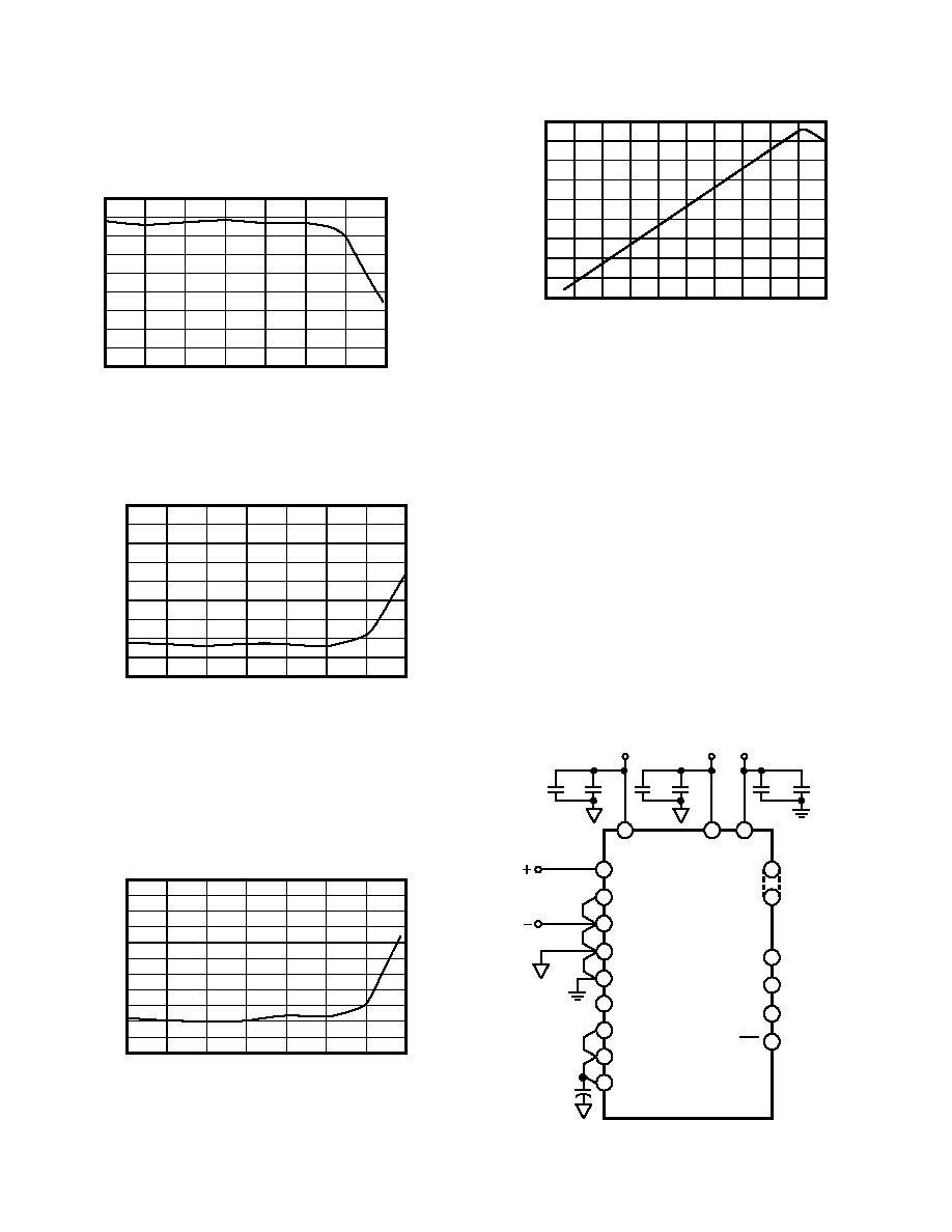
APPLYING THE AD1671
GROUNDING AND DECOUPLING RULES
Proper grounding and decoupling should be a primary design
objective in any high speed, high resolution system. The
AD1671 separates analog and digital grounds to optimize the
management of analog and digital ground currents in a system.
The AD1671 is designed to minimize the current flowing from
REF COM (Pin 20) by directing the majority of the current
from VCC (+5 V–Pin 28) to VEE (–5 V–Pin 1). Minimizing ana-
log ground currents hence reduces the potential for large ground
voltage drops. This can be especially true in systems that do not
utilize ground planes or wide ground runs. REF COM is also
configured to be code independent, therefore reducing input de-
pendent analog ground voltage drops and errors. Code depen-
dent ground current is diverted to ACOM (Pin 27). Also critical
in any high speed digital design is the use of proper digital
grounding techniques to avoid potential CMOS “ground
bounce.” Figure 3 is provided to assist in the proper layout,
grounding and decoupling techniques.
AIN1
REF IN
BPO/UPO
ACOM
BIT 1
BIT 12
DCOM
AD1671
ENCODE
DAV
OTR
MSB
AGP*
DGP*
+5V
–5V
*GROUND PLANE RECOMMENDED
AIN2
REF OUT
SHA OUT
REF COM
1
F
VCC
VEE VLOGIC
V
(
±5V)
IN
1
18
28
+5V
0.1
F
10
F
23
22
20
27
19
25
26
24
21
13
2
17
16
15
14
0.1
F10F
0.1
F10F
Figure 8. AD1671 Grounding and Decoupling
Figure 4 plots both S/(N+D) and Effective Number of Bits
(ENOB) for a 100 kHz input signal sampled from 666 kHz to
1.25 MHz.
SAMPLING FREQUENCY – kHz
72.5
68
1250
68.5
70.5
714
666
69
69.5
70
71
71.5
72
1111
1000
909
833
769
S/(N+D)
–
dB
11.75
11.50
11.25
11.00
EFFECTIVE
NUMBER
OF
BITS
Figure 4. S/(N/D) vs. Sampling Frequency, fIN = 100 kHz
Figure 5 is a THD plot for a full-scale 100 kHz input signal with
the sample frequency swept from 666 kHz to 1.25 MHz.
–68
–86
1250
–84
–76
714
666
–82
–80
–78
–74
–72
–70
1111
1000
909
833
769
SAMPLING FREQUENCY – kHz
THD
–
dB
Figure 5. THD vs. Sampling Rate, fIN = 100 kHz
The AD1671’s SFDR performance is ideal for use in communi-
cation systems such as high speed modems and digital radios.
The SFDR is better than 84 dB with sample rates up to 1.11 MHz
and increases as the input signal amplitude is attenuated by ap-
proximately 3 dB. Note also the SFDR is typically better than
80 dB with input signals attenuated by up to –7 dB.
1250
714
666
1111
1000
909
833
769
SAMPLING FREQUENCY – kHz
SPURIOUS
FREE
DYNAMIC
RANGE
–
dB
–86
–68
–84
–76
–82
–80
–78
–74
–72
–70
–88
–90
Figure 6. Spurious Free Dynamic Range vs. Sampling
Rate, fIN = 100 kHz
相关PDF资料 |
PDF描述 |
|---|---|
| MS3101A22-17S | CONN RCPT 9POS FREE HNG W/SCKT |
| VI-BN1-IV-F3 | CONVERTER MOD DC/DC 12V 150W |
| VI-B04-MY | CONVERTER MOD DC/DC 48V 50W |
| IDT72811L25PFI | IC FIFO SYNC DUAL 512X9 64-TQFP |
| MS3101F28-5S | CONN RCPT 5POS FREE HNG W/SCKT |
相关代理商/技术参数 |
参数描述 |
|---|---|
| AD1671JP-REEL | 制造商:Analog Devices 功能描述:ADC Single Pipelined 1.25Msps 12-bit Parallel 28-Pin PLCC T/R 制造商:Rochester Electronics LLC 功能描述:IC, 12-BIT 1.25 MSPS ADC - Tape and Reel |
| AD1671JPZ | 制造商:Analog Devices 功能描述:ADC Single Pipelined 1.25Msps 12-bit Parallel 28-Pin PLCC |
| AD1671JQ | 功能描述:IC ADC SNGL 12BIT 28-CDIP RoHS:否 类别:集成电路 (IC) >> 数据采集 - 模数转换器 系列:- 产品培训模块:Lead (SnPb) Finish for COTS Obsolescence Mitigation Program 标准包装:250 系列:- 位数:12 采样率(每秒):1.8M 数据接口:并联 转换器数目:1 功率耗散(最大):1.82W 电压电源:模拟和数字 工作温度:-40°C ~ 85°C 安装类型:表面贴装 封装/外壳:48-LQFP 供应商设备封装:48-LQFP(7x7) 包装:管件 输入数目和类型:2 个单端,单极 |
| AD1671K | 制造商:AD 制造商全称:Analog Devices 功能描述:Complete 12-Bit 1.25 MSPS Monolithic A/D Converter |
| AD1671KP | 功能描述:IC ADC SNGL 12BIT 28PLCC RoHS:否 类别:集成电路 (IC) >> 数据采集 - 模数转换器 系列:- 产品培训模块:Lead (SnPb) Finish for COTS Obsolescence Mitigation Program 标准包装:250 系列:- 位数:12 采样率(每秒):1.8M 数据接口:并联 转换器数目:1 功率耗散(最大):1.82W 电压电源:模拟和数字 工作温度:-40°C ~ 85°C 安装类型:表面贴装 封装/外壳:48-LQFP 供应商设备封装:48-LQFP(7x7) 包装:管件 输入数目和类型:2 个单端,单极 |
发布紧急采购,3分钟左右您将得到回复。