- 您现在的位置:买卖IC网 > PDF目录10659 > AD1674ARZ (Analog Devices Inc)IC ADC 12BIT 100KSPS 28-SOIC PDF资料下载
参数资料
| 型号: | AD1674ARZ |
| 厂商: | Analog Devices Inc |
| 文件页数: | 4/12页 |
| 文件大小: | 0K |
| 描述: | IC ADC 12BIT 100KSPS 28-SOIC |
| 标准包装: | 27 |
| 位数: | 12 |
| 采样率(每秒): | 100k |
| 数据接口: | 并联 |
| 转换器数目: | 1 |
| 功率耗散(最大): | 825mW |
| 电压电源: | 双 ± |
| 工作温度: | -40°C ~ 85°C |
| 安装类型: | 表面贴装 |
| 封装/外壳: | 28-SOIC(0.295",7.50mm 宽) |
| 供应商设备封装: | 28-SOIC W |
| 包装: | 管件 |
| 输入数目和类型: | 2 个单端,单极;2 个单端,双极 |
| 产品目录页面: | 777 (CN2011-ZH PDF) |
AD1674
REV. C
–12–
C1425b–10–3/94
PRINTED
IN
U.S.A.
GROUNDING
If a single AD1674 is used with separate analog and digital
ground planes, connect the analog ground plane to AGND and
the digital ground plane to DGND keeping lead lengths as short
as possible. Then connect AGND and DGND together at the
AD1674. If multiple AD1674s are used or the AD1674 shares
analog supplies with other components, connect the analog and
digital returns together once at the power supplies rather than at
each chip. This prevents large ground loops which inductively
couple noise and allow digital currents to flow through the ana-
log system.
GENERAL MICROPROCESSOR INTERFACE
CONSIDERATIONS
A typical A/D converter interface routine involves several opera-
tions. First, a write to the ADC address initiates a conversion.
The processor must then wait for the conversion cycle to com-
plete, since most ADCs take longer than one instruction cycle to
complete a conversion. Valid data can, of course, only be read
after the conversion is complete. The AD1674 provides an out-
put signal (STS) which indicates when a conversion is in
progress. This signal can be polled by the processor by reading
it through an external three-state buffer (or other input port).
The STS signal can also be used to generate an interrupt upon
completion of a conversion, if the system timing requirements
are critical (bear in mind that the maximum conversion time of
the AD1674 is only 10 microseconds) and the processor has
other tasks to perform during the ADC conversion cycle. An-
other possible time-out method is to assume that the ADC will
take 10 microseconds to convert, and insert a sufficient number
of “no-op” instructions to ensure that 10 microseconds of pro-
cessor time is consumed.
Once it is established that the conversion is finished, the data
can be read. In the case of an ADC of 8-bit resolution (or less),
a single data read operation is sufficient. In the case of convert-
ers with more data bits than are available on the bus, a choice of
data formats is required, and multiple read operations are
needed. The AD1674 includes internal logic to permit direct in-
terface to 8-bit or 16-bit data buses, selected by the 12/8 input.
In 16-bit bus applications (12/8 HIGH) the data lines (DB11
through DB0) may be connected to either the 12 most signifi-
cant or 12 least significant hits of the data bus. The remaining
four bits should be masked in software. The interface to an 8-bit
data bus (12/8 LOW) contains the 8 MSBs (DB11 through
DB4). The odd address (A0 HIGH) contains the 4 LSBs (DB3
through DB0) in the upper half of the byte, followed by four
trailing zeroes, thus eliminating bit masking instructions.
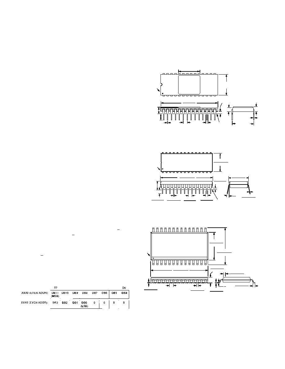
AD1674 Data Format for 8-Bit Bus
PACKAGE INFORMATION
Dimensions shown in inches and (mm).
28-Pin Ceramic DIP Package (D-28)
0.050 ±0.010
(1.27 ±0.254)
SEATING
PLANE
1.42 (36.07)
1.40 (35.56)
0.047 ±0.007
(1.19 ±0.178)
0.1 (2.54)
0.017 ±0.003
(0.43 ±0.076)
0.145 ±0.02
(3.68 ±0.51)
0.125
(3.17)
MIN
0.6 (15.24)
0.010 ±0.002
(0.254 ±0.05)
0.095
(2.41)
0.085
(2.16)
0.59 ±0.01
(14.98 ±0.254)
14
15
PIN 1
1
28
0.505 (12.83)
28-Lead Plastic DIP Package (N-28)
PIN 1
0.550 (13.97)
0.530 (13.462)
1
14
15
28
SEATING
PLANE
1.450 (38.83)
1.440 (35.576)
0.200
(5.080)
MAX
0.020 (0.508)
0.015 (0.381)
0.160 (4.06)
0.140 (3.56)
0.175 (4.45)
0.120 (3.05)
0.105 (2.67)
0.095 (2.41)
0.065 (1.65)
0.045 (1.14)
0.606 (15.39)
0.594 (15.09)
0.012 (0.305)
0.008 (0.203)
15
°
0
°
28-Lead Wide-Body SO Package (R-28)
PIN 1
0.2992 (7.60)
0.2914 (7.40)
0.4193 (10.65)
0.3937 (10.00)
1
28
15
14
0.0125 (0.32)
0.0091 (0.23)
0.0500 (1.27)
0.0157 (0.40)
8
°
0
°
0.0291 (0.74)
0.0098 (0.25)
x 45
°
0.0192 (0.49)
0.0138 (0.35)
0.0500 (1.27)
BSC
0.1043 (2.65)
0.0926 (2.35)
0.7125 (18.10)
0.6969 (17.70)
0.0118 (0.30)
0.0040 (0.10)
相关PDF资料 |
PDF描述 |
|---|---|
| AD7693BRMZ | IC ADC 16BIT 500KSPS 10-MSOP |
| VI-J1L-MW-F2 | CONVERTER MOD DC/DC 28V 100W |
| LTC1419CSW#PBF | IC A/D CONV 14BIT SAMPLNG 28SOIC |
| VI-B1L-MW | CONVERTER MOD DC/DC 28V 100W |
| VE-B1L-MX-F4 | CONVERTER MOD DC/DC 28V 75W |
相关代理商/技术参数 |
参数描述 |
|---|---|
| AD1674ARZ-REEL | 功能描述:IC ADC SINGLE 12BIT 28SOIC RoHS:是 类别:集成电路 (IC) >> 数据采集 - 模数转换器 系列:- 标准包装:1 系列:- 位数:14 采样率(每秒):83k 数据接口:串行,并联 转换器数目:1 功率耗散(最大):95mW 电压电源:双 ± 工作温度:0°C ~ 70°C 安装类型:通孔 封装/外壳:28-DIP(0.600",15.24mm) 供应商设备封装:28-PDIP 包装:管件 输入数目和类型:1 个单端,双极 |
| AD1674B | 制造商:AD 制造商全称:Analog Devices 功能描述:12-Bit 100 kSPS A/D Converter |
| AD1674BD | 功能描述:IC ADC 12BIT 100KSPS 28-CDIP RoHS:否 类别:集成电路 (IC) >> 数据采集 - 模数转换器 系列:- 标准包装:1 系列:- 位数:14 采样率(每秒):83k 数据接口:串行,并联 转换器数目:1 功率耗散(最大):95mW 电压电源:双 ± 工作温度:0°C ~ 70°C 安装类型:通孔 封装/外壳:28-DIP(0.600",15.24mm) 供应商设备封装:28-PDIP 包装:管件 输入数目和类型:1 个单端,双极 |
| AD1674BR | 功能描述:IC ADC 12BIT 100KSPS 28-SOIC RoHS:否 类别:集成电路 (IC) >> 数据采集 - 模数转换器 系列:- 标准包装:1 系列:- 位数:14 采样率(每秒):83k 数据接口:串行,并联 转换器数目:1 功率耗散(最大):95mW 电压电源:双 ± 工作温度:0°C ~ 70°C 安装类型:通孔 封装/外壳:28-DIP(0.600",15.24mm) 供应商设备封装:28-PDIP 包装:管件 输入数目和类型:1 个单端,双极 |
| AD1674BRZ | 功能描述:IC ADC 12BIT 100KSPS 28-SOIC RoHS:是 类别:集成电路 (IC) >> 数据采集 - 模数转换器 系列:- 标准包装:1 系列:microPOWER™ 位数:8 采样率(每秒):1M 数据接口:串行,SPI? 转换器数目:1 功率耗散(最大):- 电压电源:模拟和数字 工作温度:-40°C ~ 125°C 安装类型:表面贴装 封装/外壳:24-VFQFN 裸露焊盘 供应商设备封装:24-VQFN 裸露焊盘(4x4) 包装:Digi-Reel® 输入数目和类型:8 个单端,单极 产品目录页面:892 (CN2011-ZH PDF) 其它名称:296-25851-6 |
发布紧急采购,3分钟左右您将得到回复。