- 您现在的位置:买卖IC网 > PDF目录10792 > AD1851R-REEL7 (Analog Devices Inc)IC DAC AUDIO FASTSET 16B 16SOIC PDF资料下载
参数资料
| 型号: | AD1851R-REEL7 |
| 厂商: | Analog Devices Inc |
| 文件页数: | 10/12页 |
| 文件大小: | 0K |
| 描述: | IC DAC AUDIO FASTSET 16B 16SOIC |
| 标准包装: | 1 |
| 设置时间: | 1.5µs |
| 位数: | 16 |
| 数据接口: | 串行 |
| 转换器数目: | 1 |
| 电压电源: | 双 ± |
| 工作温度: | -25°C ~ 70°C |
| 安装类型: | 表面贴装 |
| 封装/外壳: | 16-SOIC(0.295",7.50mm 宽) |
| 供应商设备封装: | 16-SOIC W |
| 包装: | 标准包装 |
| 输出数目和类型: | 2 电流,双极;2 电压,双极 |
| 采样率(每秒): | * |
| 其它名称: | AD1851R-REEL7DKR |
AD1851/AD1861
REV. A
–7–
AD1851 DIGITAL CIRCUIT CONSIDERATIONS
AD1851 Input Data
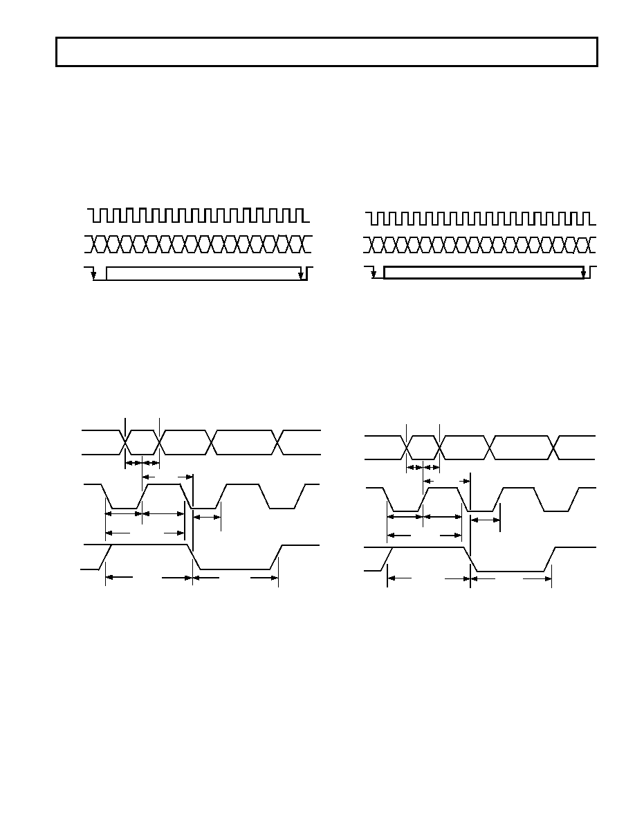
Data is transmitted to the AD1851 in a bit stream composed of
16-bit words with a serial, MSB first format. Three signals
must be present to achieve proper operation. They are the
Data, Clock and Latch Enable (LE) signals. Input data bits are
clocked into the input register on the rising edge of the Clock
signal. The LSB is clocked in on the 16th clock pulse. When all
data bits are loaded, a low-going Latch Enable pulse updates
the DAC input. Figure 5 illustrates the general signal require-
ments for data transfer to the AD1851.
DATA
CLOCK
LATCH
S
M
B
L
S
B
Figure 5. Signal Requirements for AD1851
Figure 6 illustrates the specific timing requirements that must
be met in order for the data transfer to be accomplished prop-
erly. The input pins of the AD1851 are both TTL and 5 V
CMOS compatible. The input requirements illustrated in Fig-
ures 5 and 6 are compatible with data outputs provided by
popular DSP filter chips used in digital audio playback systems.
The AD1851 input clock can run at a 12.5 MHz rate. This
clock rate will allow data transfer rates for 2 , 4
or 8
or
16
oversampling reconstructions.
>40ns
>30ns
>15ns
>40ns
DATA
CLOCK
LATCH
>15ns
>30ns
>80.0ns
>15ns
Figure 6. Timing Relationships of AD1851 Input Signals
AD1861 DIGITAL CIRCUIT CONSIDERATIONS
AD1861 Input Data
Data is transmitted to the AD1861 in a bit stream composed of
18-bit words with a serial, MSB first format. Three signals
must be present to achieve proper operation. They are the
Data, Clock and Latch Enable (LE) signals. Input data bits are
clocked into the input register on the rising edge of the Clock
signal. The LSB is clocked in on the 18th clock pulse. When all
data bits are loaded, a low-going Latch Enable pulse updates
the DAC input. Figure 7 illustrates the general signal require-
ments for data transfer to the AD1861.
DATA
CLOCK
LATCH
L
S
B
M
B
S
Figure 7. Signal Requirements for AD1861
Figure 8 illustrates the specific timing requirements that must
be met in order for the data transfer to be accomplished prop-
erly. The input pins of the AD1861 are both TTL and 5 V
CMOS compatible. The input requirements illustrated in Fig-
ures 7 and 8 are compatible with data outputs provided by
popular DSP filter chips used in digital audio playback systems.
The AD1861 input clock can run at a 13.5 MHz rate. This
clock rate will allow data transfer rates for 2 , 4
or 8
or
16
oversampling reconstructions.
>40ns
>30ns
>15ns
>40ns
DATA
CLOCK
LATCH
>15ns
>30ns
>74.1ns
>15ns
Figure 8. Timing Relationships of AD1861 Input Signals
相关PDF资料 |
PDF描述 |
|---|---|
| VI-BN1-MX-F2 | CONVERTER MOD DC/DC 12V 75W |
| CMP401GSZ | IC COMPARATOR LV 23NS 16-SOIC |
| AD5432YRM-REEL7 | IC DAC 10BIT MULTIPLYING 10-MSOP |
| VI-BN1-MX-F1 | CONVERTER MOD DC/DC 12V 75W |
| VE-BT4-IV-S | CONVERTER MOD DC/DC 48V 150W |
相关代理商/技术参数 |
参数描述 |
|---|---|
| AD1851RZ | 功能描述:IC DAC AUDIO 16BIT PCM 16-SOIC RoHS:是 类别:集成电路 (IC) >> 数据采集 - 数模转换器 系列:- 产品培训模块:Lead (SnPb) Finish for COTS Obsolescence Mitigation Program 标准包装:50 系列:- 设置时间:4µs 位数:12 数据接口:串行 转换器数目:2 电压电源:单电源 功率耗散(最大):- 工作温度:-40°C ~ 85°C 安装类型:表面贴装 封装/外壳:8-TSSOP,8-MSOP(0.118",3.00mm 宽) 供应商设备封装:8-uMAX 包装:管件 输出数目和类型:2 电压,单极 采样率(每秒):* 产品目录页面:1398 (CN2011-ZH PDF) |
| AD1851RZ-J | 功能描述:IC DAC AUDIO FASTSET 16B 16SOIC RoHS:是 类别:集成电路 (IC) >> 数据采集 - 数模转换器 系列:- 标准包装:1 系列:- 设置时间:4.5µs 位数:12 数据接口:串行,SPI? 转换器数目:1 电压电源:单电源 功率耗散(最大):- 工作温度:-40°C ~ 125°C 安装类型:表面贴装 封装/外壳:8-SOIC(0.154",3.90mm 宽) 供应商设备封装:8-SOICN 包装:剪切带 (CT) 输出数目和类型:1 电压,单极;1 电压,双极 采样率(每秒):* 其它名称:MCP4921T-E/SNCTMCP4921T-E/SNRCTMCP4921T-E/SNRCT-ND |
| AD1851RZ-REEL7 | 功能描述:IC DAC AUDIO FASTSET 16B 16SOIC RoHS:是 类别:集成电路 (IC) >> 数据采集 - 数模转换器 系列:- 产品培训模块:Lead (SnPb) Finish for COTS Obsolescence Mitigation Program 标准包装:50 系列:- 设置时间:4µs 位数:12 数据接口:串行 转换器数目:2 电压电源:单电源 功率耗散(最大):- 工作温度:-40°C ~ 85°C 安装类型:表面贴装 封装/外壳:8-TSSOP,8-MSOP(0.118",3.00mm 宽) 供应商设备封装:8-uMAX 包装:管件 输出数目和类型:2 电压,单极 采样率(每秒):* 产品目录页面:1398 (CN2011-ZH PDF) |
| AD1852 | 制造商:AD 制造商全称:Analog Devices 功能描述:Stereo, 24-Bit, 192 kHz Multibit DAC |
发布紧急采购,3分钟左右您将得到回复。