参数资料
| 型号: | AD1854JRSZ |
| 厂商: | Analog Devices Inc |
| 文件页数: | 9/12页 |
| 文件大小: | 0K |
| 描述: | IC DAC STEREO 96KHZ 5V 28SSOP |
| 产品培训模块: | Interfacing AV Converters to Blackfin Processors Data Converter Fundamentals DAC Architectures |
| 标准包装: | 47 |
| 位数: | 20 |
| 数据接口: | DSP,I²S,串行 |
| 转换器数目: | 2 |
| 电压电源: | 模拟和数字 |
| 功率耗散(最大): | 250mW |
| 工作温度: | 0°C ~ 70°C |
| 安装类型: | 表面贴装 |
| 封装/外壳: | 28-SSOP(0.209",5.30mm 宽) |
| 供应商设备封装: | 28-SSOP |
| 包装: | 管件 |
| 输出数目和类型: | 4 电压,单极 |
| 采样率(每秒): | 96k |
| 产品目录页面: | 781 (CN2011-ZH PDF) |
–6–
AD1854
REV. A
OPERATING FEATURES
Serial Data Input Port
The AD1854’s flexible serial data input port accepts data in
twos-complement, MSB-first format. The left channel data field
always precedes the right channel data field. The input data
consists of either 16, 18, 20, or 24 bits, as established by the
mode select pins (IDPM0 Pin 21 and IDPM1 Pin 20) or the
mode select bits (Bits 15 and 14) in the control register through
the SPI (Serial Peripheral Interface) control port. Neither the
pins nor the SPI controls has preference; to ensure proper control,
the selection not being used should be tied LO. Therefore,
when the SPI bits are used to control Serial Data Input Format,
Pins 20 and 21 should be tied LO. Similarly, when the pins are
to be used to select the Data Format, the SPI bits should be set
to zeros. When the SPI Control Port is not being used, the SPI
Pins (3, 4, and 5) should be tied LO.
Serial Data Input Mode
The AD1854 uses two multiplexed input pins to control the
mode configuration of the input data port mode as follows:
Table I. Serial Data Input Modes
IDPM1
IDPM0
(Pin 20)
(Pin 21)
Serial Data Input Format
0
Right Justified (16 Bits)
01
I
2S-Compatible
1
0
Right Justified (20 Bits)
1
Right Justified (24 Bits)
Bit Clock
0
Left Justified
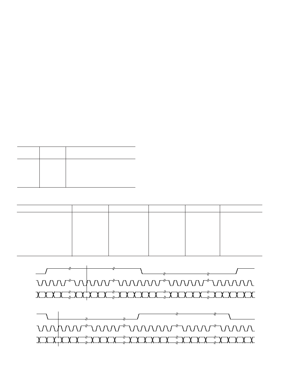
Figure 1 shows the right-justified mode (16-bit mode). L/RCLK
is HI for the left channel, LO for the right channel. Data is valid
on the rising edge of BCLK. The MSB is delayed 16-bit clock
periods from an L/RCLK transition, so that when there are 64
BCLK periods per L/RCLK period, the LSB of the data will be
right justified to the next L/RCLK transition. The right-justified
mode can also be used with 20-bit or 24-bit inputs as selected
in Table I.
Figure 2 shows the I
2S-justified mode. L/RCLK is LO for the
left channel and HI for the right channel. Data is valid on the
rising edge of BCLK. The MSB is left justified to an L/RCLK
transition but with a single BCLK period delay. The I
2S-justified
mode can be used with 16-/18-/20- or 24-bit inputs.
Figure 3 shows the left-justified mode. Note: Left-justified mode
is selected by pulsing IDPM1 (Pin 20) with bit clock, that is, tying
bit clock to IDPM1 while IDPM0 (Pin 21) is tied LO. Left-
justified can only be selected this way, it cannot be selected through
SPI Control Port.
L/RCLK is HI for the left channel, and LO for the right channel.
Data is valid on the rising edge of BCLK. The MSB is left-
justified to an L/RCLK transition, with no MSB delay. The
left-justified mode can be used with 16-/18-/20- or 24-bit inputs.
Note that the AD1854 is capable of a 32
× F
S BCLK frequency
“packed mode” where the MSB is left-justified to an L/RCLK
transition, and the LSB is right-justified to an L/RCLK transi-
tion. L/RCLK is HI for the left channel, and LO for the right
channel. Data is valid on the rising edge of BCLK. Packed
mode can be used when the AD1854 is programmed in right-
justified mode. Packed mode is shown is Figure 4.
Table II. Frequency Mode Settings
FS
96/48
MCLK
X2MCLK
384/256
Note
Normal, 32 kHz–48 kHz
0
256
× FS
00
Normal, 32 kHz–48 kHz
0
384
× F
S
01
Normal, 32 kHz–48 kHz
0
512
× FS
10
Normal, 32 kHz–48 kHz
0
1
Not Allowed
Double FS (96 kHz)
1
128
× F
S
00
Double FS (96 kHz)
1
(384/2)
× FS
01
Double FS (96 kHz)
1
256
× FS
10
Double FS (96 kHz)
1
Not Allowed
SDATA
INPUT
LSB
MSB–2
MSB–1
LSB+2 LSB+1
MSB–2
MSB–1
MSB
LSB+2 LSB+1
LSB
BCLK
INPUT
L/
RCLK
INPUT
LEFT CHANNEL
RIGHT CHANNEL
MSB
LSB
Figure 1. Right-Justified Mode
LEFT CHANNEL
RIGHT CHANNEL
MSB–2
MSB–1
LSB+2
LSB+1
LSB
MSB–2
MSB–1
MSB
LSB+2
LSB+1
LSB
MSB
L/
RCLK
INPUT
BCLK
INPUT
SDATA
INPUT
MSB
Figure 2. I2S-Justified Mode
相关PDF资料 |
PDF描述 |
|---|---|
| MS3452W28-15S | CONN RCPT 35POS BOX MNT W/SCKT |
| MS3452L28-15S | CONN RCPT 35POS BOX MNT W/SCKT |
| MS27472T18B96SA | CONN RCPT 9POS WALL MT W/SCKT |
| AD9709ASTZ | IC DAC 8BIT DUAL 125MSPS 48-LQFP |
| MS27467T25F19PD | CONN PLUG 19POS STRAIGHT W/PINS |
相关代理商/技术参数 |
参数描述 |
|---|---|
| AD1854JRSZRL | 功能描述:IC DAC STEREO 96KHZ 5V 28SSOP RoHS:是 类别:集成电路 (IC) >> 数据采集 - 数模转换器 系列:- 标准包装:47 系列:- 设置时间:2µs 位数:14 数据接口:并联 转换器数目:1 电压电源:单电源 功率耗散(最大):55µW 工作温度:-40°C ~ 85°C 安装类型:表面贴装 封装/外壳:28-SSOP(0.209",5.30mm 宽) 供应商设备封装:28-SSOP 包装:管件 输出数目和类型:1 电流,单极;1 电流,双极 采样率(每秒):* |
| AD1854KRS | 制造商:Analog Devices 功能描述:DAC 2-CH Delta-Sigma 24-bit 28-Pin SSOP 制造商:Rochester Electronics LLC 功能描述:STEREO,96KHZ, MULTIBIT SIGMA DELTA DAC - Bulk |
| AD1854KRSRL | 制造商:Analog Devices 功能描述:DAC 2-CH Delta-Sigma 24-bit 28-Pin SSOP T/R 制造商:Analog Devices 功能描述:DAC 2CH DELTA-SIGMA 24BIT 28SSOP - Tape and Reel 制造商:Rochester Electronics LLC 功能描述:STEREO,96KHZ, MULTIBIT SIGMA DELTA DAC - Tape and Reel |
| AD1855 | 制造商:AD 制造商全称:Analog Devices 功能描述:Stereo, 96 kHz, Multibit DAC |
发布紧急采购,3分钟左右您将得到回复。