参数资料
| 型号: | AD2S1205WSTZ |
| 厂商: | Analog Devices Inc |
| 文件页数: | 17/20页 |
| 文件大小: | 0K |
| 描述: | IC CONV R/D 12BIT W/OSC 44-LQFP |
| 标准包装: | 1 |
| 类型: | R/D 转换器 |
| 分辨率(位): | 12 b |
| 数据接口: | 串行,并联 |
| 电压电源: | 模拟和数字 |
| 电源电压: | 4.75 V ~ 5.25 V |
| 工作温度: | -40°C ~ 125°C |
| 安装类型: | 表面贴装 |
| 封装/外壳: | 44-LQFP |
| 供应商设备封装: | 44-LQFP(7x7) |
| 包装: | 托盘 |
| 产品目录页面: | 790 (CN2011-ZH PDF) |
AD2S1205
Rev. A | Page 6 of 20
06
33
9-
0
02
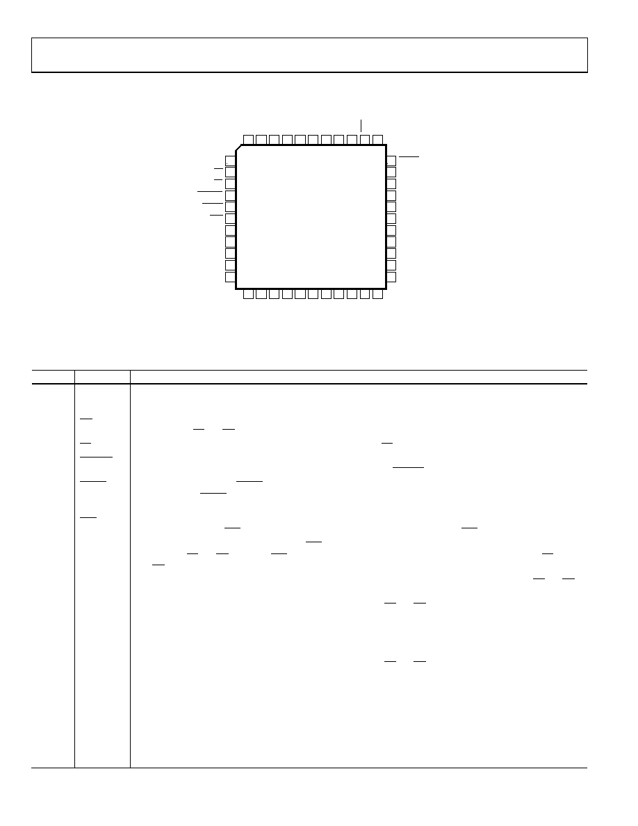
PIN CONFIGURATION AND FUNCTION DESCRIPTIONS
RE
F
O
UT
44
RE
F
BY
P
43
Co
sL
O
40
Si
n
L
O
38
AG
ND
42
AG
ND
36
AV
DD
39
EX
C
35
EX
C
34
Co
s
41
Si
n
37
DVDD 1
RD
2
CS
3
SAMPLE
4
RDVEL
5
SOE
6
DB11/SO
7
DB10/SCLK
8
DB9
9
DB8 10
DB7 11
RESET
33
FS2
32
FS1
31
LOT
30
DOS
29
AD2S1205
TOP VIEW
(Not to Scale)
DIR
28
NM
27
B
26
A
25
CPO
24
DGND
23
DB6
12
DB5
13
DB4
14
DB3
15
DG
ND
16
DV
DD
17
DB2
18
DB1
19
DB0
20
X
TA
L
O
U
T
21
CL
KI
N
22
Figure 2. Pin Configuration
Table 3. Pin Function Descriptions
Pin No.
Mnemonic
Description
1, 17
DVDD
Digital Supply Voltage, 4.75 V to 5.25 V. This is the supply voltage for all digital circuitry on the AD2S1205. The
AVDD and DVDD voltages ideally should be at the same potential and must not be more than 0.3 V apart, even
on a transient basis.
2
RD
Edge-Triggered Logic Input. This pin acts as a frame synchronization signal and output enable. The output buffer is
enabled when CS and RD are held low.
3
CS
Chip Select. Active low logic input. The device is enabled when CS is held low.
4
SAMPLE
Sample Result. Logic input. Data is transferred from the position and velocity integrators to the position and
velocity registers, respectively, after a high-to-low transition on the SAMPLE signal.
5
RDVEL
Read Velocity. Logic input. RDVEL input is used to select between the angular position register and the angular
velocity register. RDVEL is held high to select the angular position register and low to select the angular
velocity register.
6
SOE
Serial Output Enable. Logic input. This pin enables either the parallel or serial interface. The serial interface is
selected by holding the SOE pin low, and the parallel interface is selected by holding the SOE pin high.
7
DB11/SO
Data Bit 11/Serial Data Output Bus. When the SOE pin is high, this pin acts as DB11, a three-state data output pin
controlled by CS and RD. When the SOE pin is low, this pin acts as SO, the serial data output bus controlled by CS
and RD. The bits are clocked out on the rising edge of SCLK.
8
DB10/SCLK
Data Bit 10/Serial Clock. In parallel mode this pin acts as DB10, a three-state data output pin controlled by CS and RD.
In serial mode this pin acts as the serial clock input.
9 to 15
DB9 to DB3
Data Bit 9 to Data Bit 3. Three-state data output pins controlled by CS and RD.
16, 23
DGND
Digital Ground. These pins are ground reference points for digital circuitry on the AD2S1205. All digital input
signals should be referred to this DGND voltage. Both of these pins can be connected to the AGND plane of a
system. The DGND and AGND voltages should ideally be at the same potential and must not be more than 0.3 V
apart, even on a transient basis.
18 to 20
DB2 to DB0
Data Bit 2 to Data Bit 0. Three-state data output pins controlled by CS and RD.
21
XTALOUT
Crystal Output. To achieve the specified dynamic performance, an external crystal is recommended at the CLKIN and
XTALOUT pins. The position and velocity accuracy are guaranteed for a frequency range of 8.192 MHz ± 25%.
22
CLKIN
Clock Input. To achieve the specified dynamic performance, an external crystal is recommended at the CLKIN and
XTALOUT pins. The position and velocity accuracy are guaranteed for a frequency range of 8.192 MHz ± 25%.
24
CPO
Charge-Pump Output. Analog output. A 204.8 kHz square wave output with a 50% duty cycle is available at the
CPO output pin. This square wave output can be used for negative rail voltage generation or to create a VCC rail.
25
A
Incremental Encoder Emulation Output A. Logic output. This output is free running and is valid if the resolver format
input signals applied to the converter are valid.
相关PDF资料 |
PDF描述 |
|---|---|
| VE-25Z-MX-S | CONVERTER MOD DC/DC 2V 30W |
| CS3106A-36-54S | CONN PLUG 39POS STRAIGHT W/SCKT |
| VI-B14-IU-S | CONVERTER MOD DC/DC 48V 200W |
| VE-B1H-IU-S | CONVERTER MOD DC/DC 52V 200W |
| VE-25Z-MW-S | CONVERTER MOD DC/DC 2V 40W |
相关代理商/技术参数 |
参数描述 |
|---|---|
| AD2S1205YSTZ | 功能描述:IC ADC R/D 12BIT W/OSC 44-LQFP RoHS:是 类别:集成电路 (IC) >> 数据采集 - ADCs/DAC - 专用型 系列:- 产品培训模块:Lead (SnPb) Finish for COTS Obsolescence Mitigation Program 标准包装:50 系列:- 类型:数据采集系统(DAS) 分辨率(位):16 b 采样率(每秒):21.94k 数据接口:MICROWIRE?,QSPI?,串行,SPI? 电压电源:模拟和数字 电源电压:1.8 V ~ 3.6 V 工作温度:-40°C ~ 85°C 安装类型:表面贴装 封装/外壳:40-WFQFN 裸露焊盘 供应商设备封装:40-TQFN-EP(6x6) 包装:托盘 |
| AD2S1210 | 制造商:AD 制造商全称:Analog Devices 功能描述:Variable Resolution, 10-Bit to 16-Bit R/D Converter with Reference Oscillator |
| AD2S1210ASTZ | 功能描述:IC CONV R/D 10-16BIT 48-LQFP RoHS:是 类别:集成电路 (IC) >> 数据采集 - ADCs/DAC - 专用型 系列:- 产品培训模块:Lead (SnPb) Finish for COTS Obsolescence Mitigation Program 标准包装:50 系列:- 类型:数据采集系统(DAS) 分辨率(位):16 b 采样率(每秒):21.94k 数据接口:MICROWIRE?,QSPI?,串行,SPI? 电压电源:模拟和数字 电源电压:1.8 V ~ 3.6 V 工作温度:-40°C ~ 85°C 安装类型:表面贴装 封装/外壳:40-WFQFN 裸露焊盘 供应商设备封装:40-TQFN-EP(6x6) 包装:托盘 |
| AD2S1210ASTZ-RL7 | 功能描述:IC CONV R/D 10-16BIT OSC 48LQFP RoHS:是 类别:集成电路 (IC) >> 数据采集 - ADCs/DAC - 专用型 系列:- 产品培训模块:Lead (SnPb) Finish for COTS Obsolescence Mitigation Program 标准包装:50 系列:- 类型:数据采集系统(DAS) 分辨率(位):16 b 采样率(每秒):21.94k 数据接口:MICROWIRE?,QSPI?,串行,SPI? 电压电源:模拟和数字 电源电压:1.8 V ~ 3.6 V 工作温度:-40°C ~ 85°C 安装类型:表面贴装 封装/外壳:40-WFQFN 裸露焊盘 供应商设备封装:40-TQFN-EP(6x6) 包装:托盘 |
| AD2S1210BSTZ | 功能描述:IC CONV R/D 10-16BIT 48-LQFP RoHS:是 类别:集成电路 (IC) >> 数据采集 - ADCs/DAC - 专用型 系列:- 产品培训模块:Lead (SnPb) Finish for COTS Obsolescence Mitigation Program 标准包装:50 系列:- 类型:数据采集系统(DAS) 分辨率(位):16 b 采样率(每秒):21.94k 数据接口:MICROWIRE?,QSPI?,串行,SPI? 电压电源:模拟和数字 电源电压:1.8 V ~ 3.6 V 工作温度:-40°C ~ 85°C 安装类型:表面贴装 封装/外壳:40-WFQFN 裸露焊盘 供应商设备封装:40-TQFN-EP(6x6) 包装:托盘 |
发布紧急采购,3分钟左右您将得到回复。