- 您现在的位置:买卖IC网 > PDF目录1889 > AD2S1210ASTZ-RL7 (Analog Devices Inc)IC CONV R/D 10-16BIT OSC 48LQFP PDF资料下载
参数资料
| 型号: | AD2S1210ASTZ-RL7 |
| 厂商: | Analog Devices Inc |
| 文件页数: | 11/36页 |
| 文件大小: | 0K |
| 描述: | IC CONV R/D 10-16BIT OSC 48LQFP |
| 标准包装: | 500 |
| 类型: | R/D 转换器 |
| 分辨率(位): | * |
| 数据接口: | 串行,并联 |
| 电压电源: | 模拟和数字 |
| 电源电压: | 4.75 V ~ 5.25 V |
| 工作温度: | -40°C ~ 85°C |
| 安装类型: | 表面贴装 |
| 封装/外壳: | 48-LQFP |
| 供应商设备封装: | 48-LQFP(7x7) |
| 包装: | 带卷 (TR) |
第1页第2页第3页第4页第5页第6页第7页第8页第9页第10页当前第11页第12页第13页第14页第15页第16页第17页第18页第19页第20页第21页第22页第23页第24页第25页第26页第27页第28页第29页第30页第31页第32页第33页第34页第35页第36页
AD2S1210
Rev. A | Page 19 of 36
48 47
RE
F
O
UT
46
RE
F
BY
P
45
CO
S
44
CO
S
L
O
43
AV
DD
42
SI
N
L
O
41
SI
N
40
AG
ND
39
EX
C
38
EX
C
37
35
34
33
30
31
32
36
29
28
27
25
26
2
3
4
7
CLKIN
6
DVDD
5
DGND
1
8
XTALOUT
9
10
12
11
13 14 15 16 17 18
V
DRI
V
E
19
DG
ND
20 21 22 23 24
AD2S1210
07
46
7-
02
5
20pF
8.192
MHZ
4.7F
10nF
5V
10nF
10F
4.7F
10nF
BUFFER
CIRCUIT
BUFFER
CIRCUIT
S2
R2
S4
S3
S1
R1
10nF
VDRIVE
4.7F
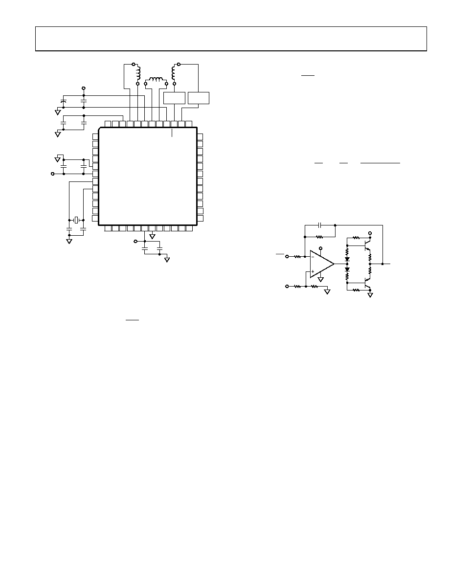
Figure 27 shows a suggested buffer circuit. Capacitor C1 may be
used in parallel with Resistor R2 to filter out any noise that may
exist on the EXC and EXC outputs. Care should be taken when
selecting the cutoff frequency of this filter to ensure that phase
shifts of the carrier caused by the filter do not exceed the phase
lock range of the AD2S1210.
The gain of the circuit is
))
1
/(
1
(
)
/
(
ω
C1
R2
R1
R2
Gain
Carrier
×
+
×
=
(7)
and
IN
REF
OUT
V
C1
R2
R1
R2
R1
R2
V
×
+
×
+
×
=
ω
1
(8)
where:
ω is the radian frequency of the applied signal.
VREF, a dc voltage, is set so that VOUT is always a positive value,
eliminating the need for a negative supply.
C1
R2
R1
12V
5V
EXC/EXC
(VIN)
(VREF)
VOUT
07
46
7-
02
6
AD8662
Figure 26. Connecting the AD2S1210 to a Resolver
In this recommended configuration, the converter introduces a
VREF/2 offset in the SIN, SINLO, COS, and COSLO signal outputs
from the resolver. The sine and cosine signals can each be
connected to a different potential relative to ground if the sine
and cosine signals adhere to the recommended specifications.
Note that because the EXC and EXC outputs are differential,
there is an inherent gain of 2×.
Figure 27. Buffer Circuit
A separate screened twisted pair cable is recommended for the
analog input pins, SIN, SINLO, COS, and COSLO. The screens
should terminate to either REFOUT or AGND.
相关PDF资料 |
PDF描述 |
|---|---|
| AD2S44-UM18B | IC CONV SYNC/R-D 14BIT 2CH 32DIP |
| AD2S80AUD | IC R/D CONV TRACKING 40CDIP |
| AD2S83APZ-REEL | IC CONV R/D MONO VAR RES 44PLCC |
| AD2S90AP | IC R/D CONV 12BIT 20-PLCC |
| AD364RJD | IC ACQ DATA 16CH 12BIT 32-CDIP |
相关代理商/技术参数 |
参数描述 |
|---|---|
| AD2S1210BSTZ | 功能描述:IC CONV R/D 10-16BIT 48-LQFP RoHS:是 类别:集成电路 (IC) >> 数据采集 - ADCs/DAC - 专用型 系列:- 产品培训模块:Lead (SnPb) Finish for COTS Obsolescence Mitigation Program 标准包装:50 系列:- 类型:数据采集系统(DAS) 分辨率(位):16 b 采样率(每秒):21.94k 数据接口:MICROWIRE?,QSPI?,串行,SPI? 电压电源:模拟和数字 电源电压:1.8 V ~ 3.6 V 工作温度:-40°C ~ 85°C 安装类型:表面贴装 封装/外壳:40-WFQFN 裸露焊盘 供应商设备封装:40-TQFN-EP(6x6) 包装:托盘 |
| AD2S1210BSTZ-DASSAULT | 制造商:Analog Devices 功能描述: |
| AD2S1210CSTZ | 功能描述:IC CONV R/D VAR RES OSC 48-LQFP RoHS:是 类别:集成电路 (IC) >> 数据采集 - ADCs/DAC - 专用型 系列:- 产品培训模块:Lead (SnPb) Finish for COTS Obsolescence Mitigation Program 标准包装:50 系列:- 类型:数据采集系统(DAS) 分辨率(位):16 b 采样率(每秒):21.94k 数据接口:MICROWIRE?,QSPI?,串行,SPI? 电压电源:模拟和数字 电源电压:1.8 V ~ 3.6 V 工作温度:-40°C ~ 85°C 安装类型:表面贴装 封装/外壳:40-WFQFN 裸露焊盘 供应商设备封装:40-TQFN-EP(6x6) 包装:托盘 |
| AD2S1210DSTZ | 功能描述:IC CONV R/D VAR RES OSC 48LQFP RoHS:是 类别:集成电路 (IC) >> 数据采集 - ADCs/DAC - 专用型 系列:- 产品培训模块:Lead (SnPb) Finish for COTS Obsolescence Mitigation Program 标准包装:50 系列:- 类型:数据采集系统(DAS) 分辨率(位):16 b 采样率(每秒):21.94k 数据接口:MICROWIRE?,QSPI?,串行,SPI? 电压电源:模拟和数字 电源电压:1.8 V ~ 3.6 V 工作温度:-40°C ~ 85°C 安装类型:表面贴装 封装/外壳:40-WFQFN 裸露焊盘 供应商设备封装:40-TQFN-EP(6x6) 包装:托盘 |
| AD2S1210DSTZ | 制造商:Analog Devices 功能描述:IC, ADC, 16BIT, PARALLEL, SERIAL, LQFP-4 |
发布紧急采购,3分钟左右您将得到回复。