- 您现在的位置:买卖IC网 > PDF目录11656 > AD2S80ASD (Analog Devices Inc)IC R/D CONV TRACKING 40CDIP PDF资料下载
参数资料
| 型号: | AD2S80ASD |
| 厂商: | Analog Devices Inc |
| 文件页数: | 6/20页 |
| 文件大小: | 0K |
| 描述: | IC R/D CONV TRACKING 40CDIP |
| 标准包装: | 1 |
| 类型: | R/D 转换器 |
| 输入类型: | 并联 |
| 输出类型: | 数字 |
| 接口: | 并联 |
| 电流 - 电源: | 30mA |
| 安装类型: | 通孔 |
| 封装/外壳: | 40-CDIP(0.600",15.24mm) |
| 供应商设备封装: | 40-DIP |
| 包装: | 管件 |
AD2S80A
REV. B
–14–
OSCILLATOR
(e.g., OSC1758)
C3
R3
TWISTED PAIR SCREENED CABLE
RESOLVER
S2
S4
S3
S1
R1
R2
1
2
3
4
5
6
7
31
AD2S80A
REF I/P
COS I/P
ANALOG
GND
DIGITAL
GND
SIGNAL
GND
SIN I/P
POWER RETURN
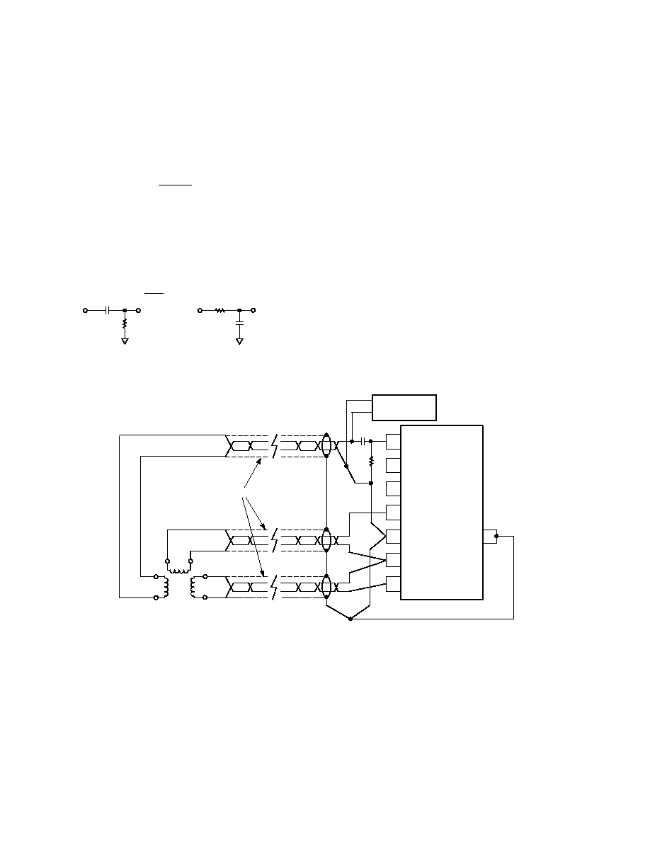
Figure 7. Connecting the AD2S80A to a Resolver
CONNECTING THE RESOLVER
The recommended connection circuit is shown in Figure 7.
In cases where the reference phase relative to the input signals
from the resolver requires adjustment, this can be easily
achieved by varying the value of the resistor R2 of the HF filter
(see Figure 1).
Assuming that R1 = R2 = R and C1 = C2 = C
and Reference Frequency =
1
2
π RC
by altering the value of R2, the phase of the reference relative to
the input signals will change in an approximately linear manner
for phase shifts of up to 10 degrees.
Increasing R2 by 10% introduces a phase lag of 2 degrees.
Decreasing R2 by 10% introduces a phase lead of 2 degrees.
C
R
PHASE LEAD = ARC TAN
1
2 fRC
R
C
PHASE LAG = ARC TAN 2 fRC
Phase Shift Circuits
TYPICAL CIRCUIT CONFIGURATION
Figure 8 shows a typical circuit configuration for the AD2S80A
in a 12-bit resolution mode. Values of the external components
have been chosen for a reference frequency of 5 kHz and a
maximum tracking rate of 260 rps with a bandwidth of 520 Hz.
Placing the values for R4, R6, C4 and C5 in the equation for KA
gives a value of 1.67
× 106. The resistors are 0.125 W, 5% toler-
ance preferred values. The capacitors are 100 V ceramic, 10%
tolerance components.
For signal and reference voltages greater than 2 V rms a simple
voltage divider circuit of resistors can be used to generate the
correct signal level at the converter. Care should be taken to
ensure that the ratios of the resistors between the sine signal line
and ground and the cosine signal line and ground are the same.
Any difference will result in an additional position error.
For more information on resistive scaling of SIN, COS and
REFERENCE converter inputs refer to the application note,
“Circuit Applications of the 2S81 and 2S81 Resolver-to-Digital
Converters.”
RELIABILITY
The AD2S80A Mean Time Between Failures (MTBF) has been
calculated according to MIL-HDBK-217E, Figure 10 shows the
MTBF in hours in naval sheltered conditions for AD2S80A/
883B only.
C
相关PDF资料 |
PDF描述 |
|---|---|
| AD2S82ALP | IC R/D CONV TRACKING 44PLCC |
| AD2S80ALD | IC R/D CONV TRACKING 40CDIP |
| D38999/26JD97PD | CONN PLUG 12POS STRAIGHT W/PINS |
| D38999/26MB5HA | CONN PLUG 5POS STRAIGHT W/PINS |
| D38999/20KA98PN | CONN RCPT 3POS WALL MNT W/PINS |
相关代理商/技术参数 |
参数描述 |
|---|---|
| AD2S80ASD/883B | 功能描述:数据转换 IC - 多种 40 PIN DIP 8 ARC MIN 883B RoHS:否 制造商:Texas Instruments 转换器数量:1 分辨率:8 bit 工作电源电压:2.7 V to 5.5 V 功耗: 工作温度范围:- 40 C to + 85 C 封装 / 箱体:MSOP-10 封装:Reel |
| AD2S80ASD883B | 制造商:AD 制造商全称:Analog Devices 功能描述:Variable Resolution, Monolithic esolver-to-Digital Converter |
| AD2S80ASE | 制造商:AD 制造商全称:Analog Devices 功能描述:Variable Resolution, Monolithic Resolver-to-Digital Converter |
| AD2S80ASE/883B | 制造商:Rochester Electronics LLC 功能描述:40 PIN PLCC 8 ARC MIN 883 - Bulk |
| AD2S80ASE883B | 制造商:AD 制造商全称:Analog Devices 功能描述:Variable Resolution, Monolithic esolver-to-Digital Converter |
发布紧急采购,3分钟左右您将得到回复。