- 您现在的位置:买卖IC网 > PDF目录11657 > AD2S83IPZ (Analog Devices Inc)IC CONV R/D MONO VAR RES 44PLCC PDF资料下载
参数资料
| 型号: | AD2S83IPZ |
| 厂商: | Analog Devices Inc |
| 文件页数: | 9/19页 |
| 文件大小: | 0K |
| 描述: | IC CONV R/D MONO VAR RES 44PLCC |
| 标准包装: | 1 |
| 类型: | R/D 转换器 |
| 输入类型: | 并联 |
| 输出类型: | 数字 |
| 接口: | 并联 |
| 电流 - 电源: | 30mA |
| 安装类型: | 表面贴装 |
| 封装/外壳: | 44-LCC(J 形引线) |
| 供应商设备封装: | 44-PLCC(16.59x16.59) |
| 包装: | 管件 |
AD2S83
–17–
REV. E
Offset Errors
The limiting factor in the measuring of low or “creep” speeds is
the level of dc offset present at zero velocity. The zero velocity
dc offset at the output of the AD2S83 is a function of the input
bias current to the VCO and the value for the input resistor R6.
See “Circuit Functions and Dynamic Performance VCO.”
The offset can be minimized by reducing the maximum tracking
rate so reducing the value for R6. Offset is a function of tracking
rate and therefore resolution; the dc offset is lowest at 16 bits.
To increase the dynamic range of the velocity dynamic resolu-
tion switching can be employed. (Contact MCG Applications
for more information.)
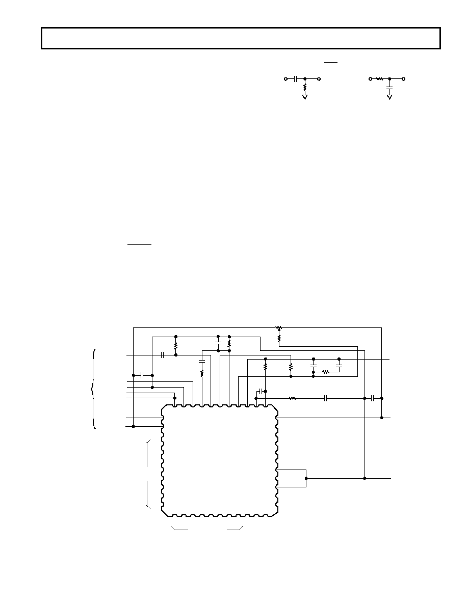
CONNECTING THE RESOLVER
The recommended connection circuit is shown in Figure 11.
In cases where the reference phase relative to the input signals
from the resolver requires adjustment, this can be easily
achieved by varying the value of the resistor R2 of the HF filter
(see Figure 1).
Assume that R1 = R2 = R and C1 = C2 = C
and Reference Frequency =
1
2
π RC
.
By altering the value of R2, the phase of the reference relative to
the input signals will change in an approximately linear manner
for phase shifts of up to 10 degrees.
Increasing R2 by 10% introduces a phase lag of two degrees.
Decreasing R2 by 10% introduces a phase lead of two degrees.
R9
1M
R8
4.7M
R2
15k
R4
130k
R6
62k
R5
200k
R7
3.3k
R3
100k
C3
100nF
C2
2.2nF
C7
150pF
C4
1.2nF
C6
390pF
C5
6.2nF
100nF
VELOCITY
O/P
–12V
0V
COS LOW
REF LOW
COS HIGH
SIN LOW
SIN HIGH
+12V
REFERENCE
INPUT
RESOLVER
SIGNAL
MSB
+5V
ENABLE
LSB
BYTE
SELECT
INHIBIT
SC2
DATA LOAD
BUSY
RIPPLE CLOCK
COMPLEMENT
DIRECTION
NOTE: R7, C6 AND C7 SHOULD BE CONNECTED AS
CLOSE AS POSSIBLE TO THE CONVERTER PINS.
SIGNAL SCREENS SHOULD BE CONNECTED TO PIN 5.
65432
1
44 43 42 41 40
18 19 20 21 22 23 24 25 26 27 28
7
8
9
10
11
12
13
14
15
16
17
39
38
37
36
35
34
33
32
31
30
29
AD2S83
TOP VIEW
(Not to Scale)
DATA
OUTPUT
DATA OUTPUT
R1
15k
C1
2.2nF
Figure 11. Typical Circuit Configuration
C
R
PHASE LEAD = ARC TAN
1
2 fRC
R
C
PHASE LAG = ARC TAN 2 fRC
PHASE SHIFT
CIRCUITS
Figure 10. Phase Shift Circuits
TYPICAL CIRCUIT CONFIGURATION
Figure 11 shows a typical circuit configuration for the AD2S83
with 12-bit resolution. Values of the external components have
been chosen for a reference frequency of 5 kHz and a maximum
tracking rate of 260 rps with a bandwidth of 520 Hz. Placing the
values for R4, R6, C4, and C5 in the equation for KA gives a
value of 1.65
× 106. The resistors are 0.125 W, 5% tolerance
preferred values. The capacitors are 100 V ceramic, 10% toler-
ance components.
For signal and reference voltages greater than 2 V rms a simple
voltage divider circuit of resistors can be used to generate the
correct signal level at the converter. Care should be taken to
ensure that the ratios of the resistors between the sine signal line
and ground and the cosine signal line and ground are the same.
Any difference will result in an additional position error.
For more information on resistive scaling of SIN, COS, and
REFERENCE converter inputs refer to the application note,
“Circuit Applications of the 2S81 and 2S80 Resolver-to-Digital
Converters.”
相关PDF资料 |
PDF描述 |
|---|---|
| VE-JNM-IY-F1 | CONVERTER MOD DC/DC 10V 50W |
| AD2S83IPZ-REEL | IC CONV R/D MONO VAR RES 44PLCC |
| AD2S82AHP | IC R/D CONV TRACKING 44PLCC |
| VE-JNL-IZ-B1 | CONVERTER MOD DC/DC 28V 25W |
| AD2S82AHP-REEL | IC CONV R/D MONO VAR RES 44PLCC |
相关代理商/技术参数 |
参数描述 |
|---|---|
| AD2S83IPZ-REEL | 功能描述:IC CONV R/D MONO VAR RES 44PLCC RoHS:是 类别:集成电路 (IC) >> 接口 - 传感器和探测器接口 系列:- 其它有关文件:Automotive Product Guide 产品培训模块:Lead (SnPb) Finish for COTS Obsolescence Mitigation Program 标准包装:74 系列:- 类型:触控式传感器 输入类型:数字 输出类型:数字 接口:JTAG,串行 电流 - 电源:100µA 安装类型:表面贴装 封装/外壳:20-TSSOP(0.173",4.40mm 宽) 供应商设备封装:20-TSSOP 包装:管件 |
| AD2S90 | 制造商:AD 制造商全称:Analog Devices 功能描述:Low Cost, Complete 12-Bit Resolver-to-Digital Converter |
| AD2S90AP | 功能描述:IC R/D CONV 12BIT 20-PLCC RoHS:否 类别:集成电路 (IC) >> 接口 - 传感器和探测器接口 系列:- 其它有关文件:Automotive Product Guide 产品培训模块:Lead (SnPb) Finish for COTS Obsolescence Mitigation Program 标准包装:74 系列:- 类型:触控式传感器 输入类型:数字 输出类型:数字 接口:JTAG,串行 电流 - 电源:100µA 安装类型:表面贴装 封装/外壳:20-TSSOP(0.173",4.40mm 宽) 供应商设备封装:20-TSSOP 包装:管件 |
| AD2S90APZ | 功能描述:IC R/D CONV 12BIT 20-PLCC RoHS:是 类别:集成电路 (IC) >> 接口 - 传感器和探测器接口 系列:- 其它有关文件:Automotive Product Guide 产品培训模块:Lead (SnPb) Finish for COTS Obsolescence Mitigation Program 标准包装:74 系列:- 类型:触控式传感器 输入类型:数字 输出类型:数字 接口:JTAG,串行 电流 - 电源:100µA 安装类型:表面贴装 封装/外壳:20-TSSOP(0.173",4.40mm 宽) 供应商设备封装:20-TSSOP 包装:管件 |
| AD2S90APZ-MOOG | 制造商:Analog Devices 功能描述: |
发布紧急采购,3分钟左右您将得到回复。