参数资料
| 型号: | AD420ARZ-32 |
| 厂商: | Analog Devices Inc |
| 文件页数: | 6/16页 |
| 文件大小: | 0K |
| 描述: | IC DAC SRL 16BIT 24-SOIC |
| 产品培训模块: | Data Converter Fundamentals DAC Architectures |
| 标准包装: | 31 |
| 设置时间: | 2.5µs |
| 位数: | 16 |
| 数据接口: | 串行 |
| 转换器数目: | 1 |
| 电压电源: | 单电源 |
| 功率耗散(最大): | 176mW |
| 工作温度: | -40°C ~ 85°C |
| 安装类型: | 表面贴装 |
| 封装/外壳: | 24-SOIC(0.295",7.50mm 宽) |
| 供应商设备封装: | 24-SOIC W |
| 包装: | 管件 |
| 输出数目和类型: | 2 电流,双极 |
| 采样率(每秒): | 400 |
| 产品目录页面: | 781 (CN2011-ZH PDF) |
AD420
Rev. H | Page 14 of 16
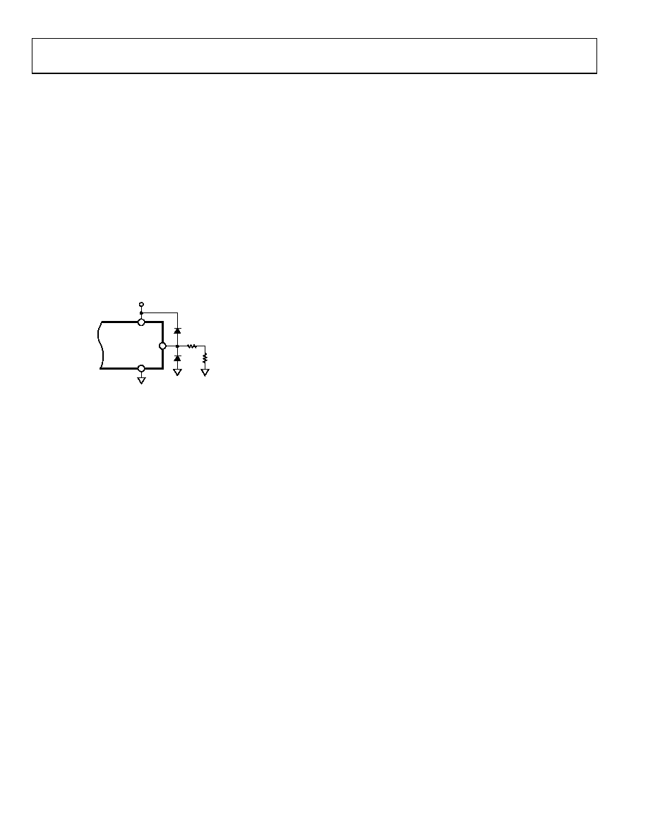
AD420 PROTECTION
TRANSIENT VOLTAGE PROTECTION
The AD420 contains ESD protection diodes, which prevent
damage from normal handling. The industrial control envir-
onment can, however, subject I/O circuits to much higher
transients. To protect the AD420 from excessively high voltage
transients, such as those specified in IEC 801, external power
diodes and a surge current limiting resistor may be required, as
shown in Figure 15. The constraint on the resistor is that during
normal operation the output voltage level at IOUT must remain
within its voltage compliance limit
(IOUT × (Rp + RLOAD) ≤ VCC 2.75 V)
and the two protection diodes and resistor must have
appropriate power ratings.
00
49
4-
0
15
AD420 I
OUT
VCC
RLOAD
RP
GND
Figure 15. Output Transient Voltage Protection
BOARD LAYOUT AND GROUNDING
The AD420 ground pin, designated GND, is the high quality
ground reference point for the device. Any external loads on the
REF OUT and VOUT pins of the AD420 should be returned to
this reference point. Analog and digital ground currents should
not share a common path. Each signal should have an appropriate
analog or digital signal return routed close to it. Using this
approach, signal loops enclose a small area, minimizing the
inductive coupling of noise. Wide PC tracks, large gauge wire,
and ground planes are highly recommended to provide low
impedance signal paths.
POWER SUPPLIES AND DECOUPLING
The AD420 supply pins, VCC (Pin 23) and VLL (Pin 2), should be
decoupled to GND with 0.1 μF capacitors to eliminate high
frequency noise that may otherwise get coupled into the analog
system. High frequency ceramic capacitors are recommended.
The decoupling capacitors should be located in close proximity
to the pins and the ground line to have maximum effect. Further
reductions in noise, and improvements in performance, may be
achieved by using a larger value capacitor on the VLL pin.
相关PDF资料 |
PDF描述 |
|---|---|
| VI-24Z-MU-F3 | CONVERTER MOD DC/DC 2V 80W |
| AD7849BRZ | IC DAC 14/16BIT SRL-IN 20-SOIC |
| VI-J4D-MZ-F1 | CONVERTER MOD DC/DC 85V 25W |
| AD8522ARZ | IC DAC 12BIT DUAL 5V 14-SOIC |
| VE-20X-MY-F2 | CONVERTER MOD DC/DC 5.2V 50W |
相关代理商/技术参数 |
参数描述 |
|---|---|
| AD420ARZ-32-REEL | 功能描述:IC DAC SERIAL INPUT 16BIT 24SOIC RoHS:是 类别:集成电路 (IC) >> 数据采集 - 数模转换器 系列:- 产品培训模块:Data Converter Fundamentals DAC Architectures 标准包装:750 系列:- 设置时间:7µs 位数:16 数据接口:并联 转换器数目:1 电压电源:双 ± 功率耗散(最大):100mW 工作温度:0°C ~ 70°C 安装类型:表面贴装 封装/外壳:28-LCC(J 形引线) 供应商设备封装:28-PLCC(11.51x11.51) 包装:带卷 (TR) 输出数目和类型:1 电压,单极;1 电压,双极 采样率(每秒):143k |
| AD421 | 制造商:AD 制造商全称:Analog Devices 功能描述:Loop-Powered 4 mA to 20 mA DAC |
| AD421-00E | 功能描述:SENSOR MAG SW 20G CROS AX 8-MSOP 制造商:nve corp/sensor products 系列:AD 包装:管件 零件状态:有效 功能:全极开关 技术:霍尔效应 极化:任意一种 感应范围:±2.5mT 跳闸,±1.1mT 释放 测试条件:-40°C ~ 125°C 电压 - 电源:4.5 V ~ 30 V 电流 - 电源(最大值):4.5mA 电流 - 输出(最大值):20mA 输出类型:开路集电极 特性:- 工作温度:-40°C ~ 125°C(TA) 封装/外壳:8-TSSOP,8-MSOP(0.118",3.00mm 宽) 供应商器件封装:8-MSOP 标准包装:1,000 |
| AD421-02E | 功能描述:SENSOR MAG SW 20G CROS AXS 8SOIC 制造商:nve corp/sensor products 系列:AD 包装:管件 零件状态:有效 功能:全极开关 技术:霍尔效应 极化:任意一种 感应范围:±2.5mT 跳闸,±1.1mT 释放 测试条件:-40°C ~ 125°C 电压 - 电源:4.5 V ~ 30 V 电流 - 电源(最大值):4.5mA 电流 - 输出(最大值):20mA 输出类型:开路集电极 特性:- 工作温度:-40°C ~ 125°C(TA) 封装/外壳:8-SOIC(0.154",3.90mm 宽) 供应商器件封装:8-SOIC 标准包装:1,000 |
| AD42124 | 制造商:Rochester Electronics LLC 功能描述:- Bulk |
发布紧急采购,3分钟左右您将得到回复。