- 您现在的位置:买卖IC网 > PDF目录8661 > AD5060BRJZ-2REEL7 (Analog Devices Inc)IC DAC 16BIT SPI/SRL SOT23-8 PDF资料下载
参数资料
| 型号: | AD5060BRJZ-2REEL7 |
| 厂商: | Analog Devices Inc |
| 文件页数: | 9/24页 |
| 文件大小: | 0K |
| 描述: | IC DAC 16BIT SPI/SRL SOT23-8 |
| 产品培训模块: | DAC Architectures |
| 标准包装: | 1 |
| 系列: | nanoDAC™ |
| 设置时间: | 4µs |
| 位数: | 16 |
| 数据接口: | DSP,MICROWIRE?,QSPI?,串行,SPI? |
| 转换器数目: | 1 |
| 电压电源: | 单电源 |
| 功率耗散(最大): | 6mW |
| 工作温度: | -40°C ~ 85°C |
| 安装类型: | 表面贴装 |
| 封装/外壳: | SOT-23-8 |
| 供应商设备封装: | SOT-23-8 |
| 包装: | 标准包装 |
| 输出数目和类型: | 1 电压,单极;1 电压,双极 |
| 采样率(每秒): | 250k |
| 其它名称: | AD5060BRJZ-2REEL7DKR |
AD5040/AD5060
Rev. A | Page 17 of 24
POWER-DOWN MODES
The AD5060 features four operating modes, and the AD5040
features three operating modes. These modes are software pro-
grammable by setting two bits in the control register (Bit DB17
and Bit DB16 in the AD5060 and Bit DB15 and Bit DB14 in the
corresponds to the operating mode of the two devices.
Table 6. Operating Modes for the AD5060
DB17
DB16
Operating Mode
0
Normal operation
Power-down modes:
0
1
3-state
1
0
100 kΩ to GND
1
1 kΩ to GND
Table 7. Operating Modes for the AD5040
DB15
DB14
Operating Mode
0
Normal operation
Power-down modes:
0
1
3-state
1
0
100 kΩ to GND
1
See Software Reset section
In both the AD5060 and the AD5040, when the two most
significant bits are set to 0, the part has normal power
consumption. However, for the three power-down modes of the
AD5060 and the two power down modes of the AD5040, the
supply current falls to less than 1μA at 5 V (65 nA at 3 V). Not
only does the supply current fall, but the output stage is also
internally switched from the output of the amplifier to a resistor
network of known values. This is advantageous because the
output impedance of the part is known while the part is in
power-down mode. The output is connected internally to GND
through a 1 kΩ resistor (AD5060 only) or a 100 kΩ resistor, or
it is left open-circuited (three-stated). The output stage is
illustrated in Figure 44.
POWER-DOWN
CIRCUITRY
AD5040/
AD5060
DAC
04767-029
VOUT
RESISTOR
NETWORK
OUTPUT
BUFFER
Figure 44. Output Stage During Power-Down
The bias generator, the DAC core, and other associated linear
circuitry are all shut down when power-down mode is
activated. However, the contents of the DAC register are
unaffected when in power-down. The time to exit power-down
is typically 2.5 μs for VDD = 5 V, and 5 μs for VDD = 3 V;
see Figure 29.
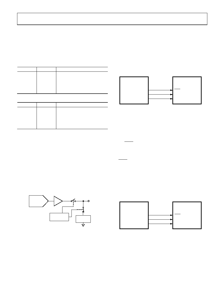
MICROPROCESSOR INTERFACING
AD5040/AD5060 to ADSP-2101/ADSP-2103 Interface
Figure 45 shows a serial interface between the AD5040/AD5060
and the ADSP-2101/ADSP-2103. The ADSP-2101/ADSP-2103
should be set up to operate in the SPORT transmit alternate
framing mode. The ADSP-2101/ADSP-2103 sport is pro-
grammed through the SPORT control register and should be
configured for internal clock operation, active low framing, and
16-bit word length. Transmission is initiated by writing a word
to the Tx register after the SPORT has been enabled.
AD5040/
AD50601
1ADDITIONAL PINS OMITTED FOR CLARITY
TFS
DT
SCLK
SYNC
DIN
SCLK
04767-030
ADSP-2101/
ADSP-21031
Figure 45. AD5040/AD5060 to ADSP-2101/ADSP-2103 Interface
AD5040/AD5060 to 68HC11/68L11 Interface
Figure 46 shows a serial interface between the AD5040/
AD5060 and the 68HC11/68L11 microcontroller. SCK of the
68HC11/68L11 drives the SCLK pin of the AD5040/AD5060,
while the MOSI output drives the serial data line of the DAC.
The SYNC signal is derived from a port line (PC7). The setup
conditions for correct operation of this interface require that the
68HC11/68L11 be configured so that its CPOL bit is 0 and its
CPHA bit is 1. When data is being transmitted to the DAC, the
SYNC line is taken low (PC7). When the 68HC11/68L11 is
configured where its CPOL bit is 0 and its CPHA bit is 1, data
appearing on the MOSI output is valid on the falling edge of
SCK. Serial data from the 68HC11/68L11 is transmitted in 8-bit
bytes with only 8 falling clock edges occurring in the transmit
cycle. Data is transmitted MSB first. In order to load data to the
AD5040/AD5060, PC7 is left low after the first eight bits are
transferred, and a second serial write operation is performed to
the DAC. PC7 is taken high at the end of this procedure.
AD5040/
AD50601
1ADDITIONAL PINS OMITTED FOR CLARITY
PC7
SCK
MOSI
SYNC
SCLK
DIN
04767-032
68HC11/
68L111
Figure 46. AD5040/AD5060 to 68HC11/68L11 Interface
相关PDF资料 |
PDF描述 |
|---|---|
| VI-J4B-MX-B1 | CONVERTER MOD DC/DC 95V 75W |
| VI-23K-MW-B1 | CONVERTER MOD DC/DC 40V 100W |
| VI-23J-MW-B1 | CONVERTER MOD DC/DC 36V 100W |
| VE-J1M-MY | CONVERTER MOD DC/DC 10V 50W |
| AD5624BCPZ-R2 | IC DAC NANO 12BIT QUAD 10-LFCSP |
相关代理商/技术参数 |
参数描述 |
|---|---|
| AD5060YRJZ-1500RL7 | 功能描述:IC DAC 16BIT SPI/SRL SOT23-8 RoHS:是 类别:集成电路 (IC) >> 数据采集 - 数模转换器 系列:nanoDAC™ 产品培训模块:Lead (SnPb) Finish for COTS Obsolescence Mitigation Program 标准包装:50 系列:- 设置时间:4µs 位数:12 数据接口:串行 转换器数目:2 电压电源:单电源 功率耗散(最大):- 工作温度:-40°C ~ 85°C 安装类型:表面贴装 封装/外壳:8-TSSOP,8-MSOP(0.118",3.00mm 宽) 供应商设备封装:8-uMAX 包装:管件 输出数目和类型:2 电压,单极 采样率(每秒):* 产品目录页面:1398 (CN2011-ZH PDF) |
| AD5060YRJZ-1REEL7 | 功能描述:IC DAC 16BIT SPI/SRL SOT23-8 RoHS:是 类别:集成电路 (IC) >> 数据采集 - 数模转换器 系列:nanoDAC™ 标准包装:47 系列:- 设置时间:2µs 位数:14 数据接口:并联 转换器数目:1 电压电源:单电源 功率耗散(最大):55µW 工作温度:-40°C ~ 85°C 安装类型:表面贴装 封装/外壳:28-SSOP(0.209",5.30mm 宽) 供应商设备封装:28-SSOP 包装:管件 输出数目和类型:1 电流,单极;1 电流,双极 采样率(每秒):* |
| AD5061 | 制造商:AD 制造商全称:Analog Devices 功能描述:Full Accurate 14/16 Bit Vout nanoDac Buffered, 3V/5V, Sot 23 |
| AD50611-1 | 制造商:Rochester Electronics LLC 功能描述:- Bulk |
| AD5061BRJZ-1 | 制造商:Analog Devices 功能描述:DAC SGL R-2R 16BIT 8PIN SOT-23 - Bulk |
发布紧急采购,3分钟左右您将得到回复。