- 您现在的位置:买卖IC网 > PDF目录9301 > AD5171BRJZ10-R2 (Analog Devices Inc)IC DGTL POT OTP 10K I2C SOT23-8 PDF资料下载
参数资料
| 型号: | AD5171BRJZ10-R2 |
| 厂商: | Analog Devices Inc |
| 文件页数: | 6/24页 |
| 文件大小: | 0K |
| 描述: | IC DGTL POT OTP 10K I2C SOT23-8 |
| 标准包装: | 1 |
| 接片: | 64 |
| 电阻(欧姆): | 10k |
| 电路数: | 1 |
| 温度系数: | 标准值 35 ppm/°C |
| 存储器类型: | 非易失 |
| 接口: | I²C(设备位址) |
| 电源电压: | 2.7 V ~ 5.5 V |
| 工作温度: | -40°C ~ 125°C |
| 安装类型: | 表面贴装 |
| 封装/外壳: | SOT-23-8 |
| 供应商设备封装: | SOT-23-8 |
| 包装: | 标准包装 |
| 配用: | AD5171EVAL-ND - BOARD EVAL FOR AD5171 |
| 其它名称: | AD5171BRJZ10-R2DKR |
AD5171
Rev. D | Page 14 of 24
Ignoring the effect of the wiper resistance, the transfer function
is simply
A
W
V
D
V
63
)
(
=
(3)
A more accurate calculation, which includes the wiper
resistance effect, yields
A
W
AB
W
AB
W
V
R
D
V
2
63
)
(
+
=
(4)
Unlike in rheostat mode where the absolute tolerance is high,
potentiometer mode yields an almost ratiometric function of
D/63 with a relatively small error contributed by the RW terms;
thus, the tolerance effect is almost cancelled. Although the thin
film step resistor (RS) and CMOS switches resistance (RW) have
very different temperature coefficients, the ratiometric adjustment
also reduces the overall temperature coefficient effect to 5 ppm/°C,
except at low value codes where RW dominates.
Potentiometer mode includes other operations such as op amp
input, feedback resistor networks, and voltage scaling applications.
Terminal A, Terminal W, and Terminal B can, in fact, be input
or output terminals provided that |VAB|, |VWA|, and |VWB| do not
exceed VDD to GND.
POWER SUPPLY CONSIDERATIONS
To minimize the package pin count, both the OTP and normal
operating voltage supplies share the same VDD terminal of the
AD5171. The AD5171 employs fuse link technology that requires
4.75 V to 5.25 V for blowing the internal fuses to achieve a
given setting, but normal VDD can be anywhere between 2.7 V
and 5.5 V after the fuse programming process. As a result, dual
voltage supplies and isolation are needed if system VDD is lower
than the required VDD_OTP. The fuse programming supply (either
an on-board regulator or rack-mount power supply) must be
rated at 4.75 V to 5.25 V and able to provide a 100 mA current
for 400 ms for successful one-time programming. Once fuse
programming is complete, the VDD_OTP supply must be removed
to allow normal operation at 2.7 V to 5.5 V; the device then
consumes current in the μA range.
03
43
7-
05
2
VDD
2.7V
5V
P1
R1
10k
P2
APPLY FOR OTP ONLY
AD5171
C2
0.1F
C1
10F
P1 = P2 = FDV302P, NDS0610
Figure 29. 5 V OTP Supply Isolated from the 2.7 V Normal Operating Supply;
the VDD_OTP supply must be removed once OTP is complete.
When operating at 2.7 V, use of the bidirectional low threshold
P-Ch MOSFETs is recommended for the isolation of the supply.
As shown in Figure 29, this assumes that the 2.7 V system
voltage is applied first, and the P1 and P2 gates are pulled to
ground, thus turning on P1 and, subsequently, P2. As a result,
VDD of the AD5171 approaches 2.7 V. When the AD5171 setting
is found, the factory tester applies the VDD_OTP to both the VDD
and the MOSFETs gates, thus turning off P1 and P2. The OTP
command should be executed at this time to program the
AD5171 while the 2.7 V source is protected. Once the fuse
programming is complete, the tester withdraws the VDD_OTP and
the setting of the AD5171 is permanently fixed.
The AD5171 achieves the OTP function through blowing
internal fuses. Users should always apply the 4.75 V to
5.25 V one-time program voltage requirement at the first
fuse programming attempt. Failure to comply with this
requirement may lead to a change in the fuse structures,
rendering programming inoperable.
Care should be taken when SCL and SDA are driven from a low
voltage logic controller. Users must ensure that the logic high
for Different Voltage Operation section.
Poor PCB layout introduces parasitics that may affect the fuse
programming. Therefore, it is recommended that a 10 μF
tantalum capacitor be added in parallel with a 1 nF ceramic
capacitor as close as possible to the VDD pin. The type and value
chosen for both capacitors are important. This combination of
capacitor values provides both a fast response and larger supply
current handling with minimum supply droop during transients.
As a result, these capacitors increase the OTP programming
success by not inhibiting the proper energy needed to blow the
internal fuses. Additionally, C1 minimizes transient disturbance
and low frequency ripple, while C2 reduces high frequency
noise during normal operation.
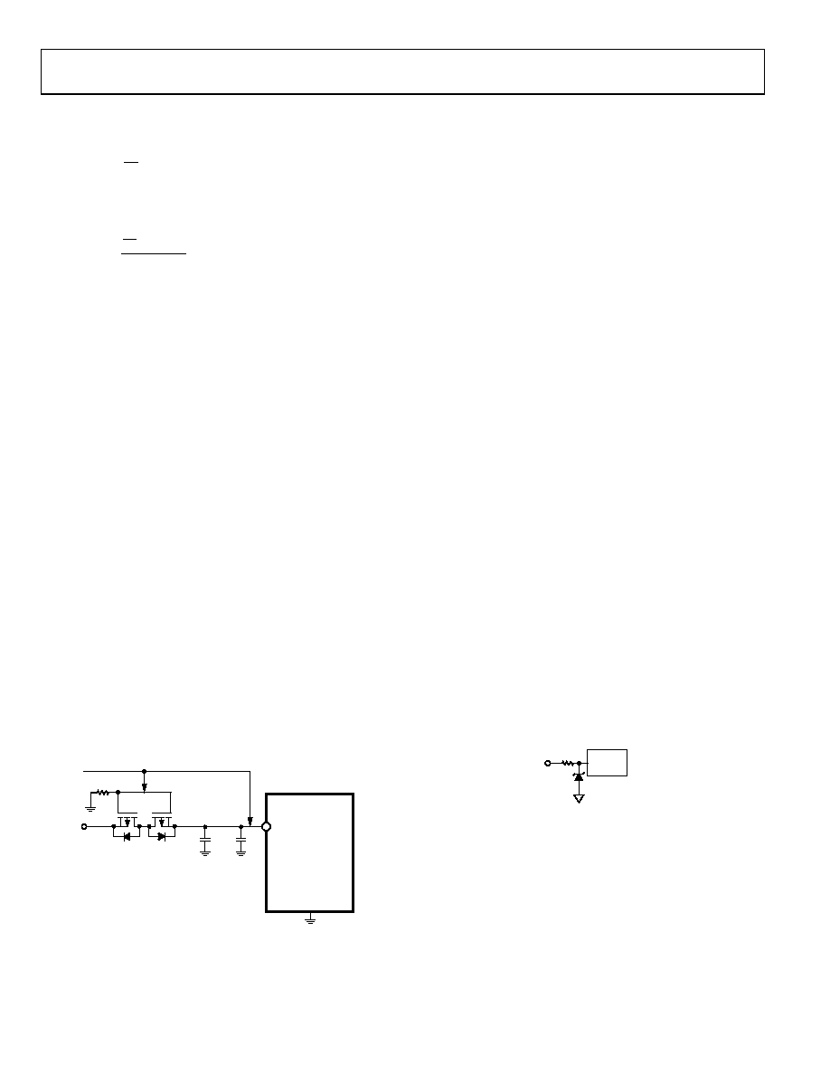
ESD PROTECTION
Digital inputs SDA and SCL are protected with a series input
resistor and parallel Zener ESD structures (see Figure 30).
LOGIC
340
GND
03
43
7
-02
7
Figure 30. ESD Protection of Digital Pins
相关PDF资料 |
PDF描述 |
|---|---|
| VI-BND-IU-F4 | CONVERTER MOD DC/DC 85V 200W |
| LTC6994HDCB-1#TRMPBF | IC DELAY LINE 6-DFN |
| LTC6994IS6-2#TRPBF | IC DELAY LINE TSOT-23-6 |
| VI-BND-IU-F3 | CONVERTER MOD DC/DC 85V 200W |
| LTC6994IS6-2#TRMPBF | IC DELAY LINE TSOT-23-6 |
相关代理商/技术参数 |
参数描述 |
|---|---|
| AD5171BRJZ10-R7 | 功能描述:IC DGTL POT OTP 10K SOT23-8 RoHS:是 类别:集成电路 (IC) >> 数据采集 - 数字电位器 系列:- 标准包装:3,000 系列:DPP 接片:32 电阻(欧姆):10k 电路数:1 温度系数:标准值 300 ppm/°C 存储器类型:非易失 接口:3 线串行(芯片选择,递增,增/减) 电源电压:2.5 V ~ 6 V 工作温度:-40°C ~ 85°C 安装类型:表面贴装 封装/外壳:8-WFDFN 裸露焊盘 供应商设备封装:8-TDFN(2x3) 包装:带卷 (TR) |
| AD5171BRJZ50-R2 | 功能描述:IC DGTL POT OTP 50K I2C SOT23-8 RoHS:是 类别:集成电路 (IC) >> 数据采集 - 数字电位器 系列:- 标准包装:3,000 系列:DPP 接片:32 电阻(欧姆):10k 电路数:1 温度系数:标准值 300 ppm/°C 存储器类型:非易失 接口:3 线串行(芯片选择,递增,增/减) 电源电压:2.5 V ~ 6 V 工作温度:-40°C ~ 85°C 安装类型:表面贴装 封装/外壳:8-WFDFN 裸露焊盘 供应商设备封装:8-TDFN(2x3) 包装:带卷 (TR) |
| AD5171BRJZ50-R7 | 功能描述:IC DGTL POT OTP 50K SOT23-8 RoHS:是 类别:集成电路 (IC) >> 数据采集 - 数字电位器 系列:- 标准包装:3,000 系列:DPP 接片:32 电阻(欧姆):10k 电路数:1 温度系数:标准值 300 ppm/°C 存储器类型:非易失 接口:3 线串行(芯片选择,递增,增/减) 电源电压:2.5 V ~ 6 V 工作温度:-40°C ~ 85°C 安装类型:表面贴装 封装/外壳:8-WFDFN 裸露焊盘 供应商设备封装:8-TDFN(2x3) 包装:带卷 (TR) |
| AD5171BRJZ5-R2 | 功能描述:IC DGTL POT OTP 5K 12C SOT23-8 RoHS:是 类别:集成电路 (IC) >> 数据采集 - 数字电位器 系列:- 标准包装:3,300 系列:WiperLock™ 接片:257 电阻(欧姆):100k 电路数:1 温度系数:标准值 150 ppm/°C 存储器类型:易失 接口:3 线 SPI(芯片选择) 电源电压:1.8 V ~ 5.5 V 工作温度:-40°C ~ 125°C 安装类型:表面贴装 封装/外壳:8-VDFN 裸露焊盘 供应商设备封装:8-DFN-EP(3x3) 包装:带卷 (TR) |
| AD5171BRJZ5-R7 | 功能描述:IC DGTL POT OTP 5K SOT23-8 RoHS:是 类别:集成电路 (IC) >> 数据采集 - 数字电位器 系列:- 标准包装:3,000 系列:DPP 接片:32 电阻(欧姆):10k 电路数:1 温度系数:标准值 300 ppm/°C 存储器类型:非易失 接口:3 线串行(芯片选择,递增,增/减) 电源电压:2.5 V ~ 6 V 工作温度:-40°C ~ 85°C 安装类型:表面贴装 封装/外壳:8-WFDFN 裸露焊盘 供应商设备封装:8-TDFN(2x3) 包装:带卷 (TR) |
发布紧急采购,3分钟左右您将得到回复。