参数资料
| 型号: | AD5171BRJZ5-R7 |
| 厂商: | Analog Devices Inc |
| 文件页数: | 11/24页 |
| 文件大小: | 0K |
| 描述: | IC DGTL POT OTP 5K SOT23-8 |
| 标准包装: | 3,000 |
| 接片: | 64 |
| 电阻(欧姆): | 5k |
| 电路数: | 1 |
| 温度系数: | 标准值 35 ppm/°C |
| 存储器类型: | 非易失 |
| 接口: | I²C(设备位址) |
| 电源电压: | 2.7 V ~ 5.5 V |
| 工作温度: | -40°C ~ 125°C |
| 安装类型: | 表面贴装 |
| 封装/外壳: | SOT-23-8 |
| 供应商设备封装: | SOT-23-8 |
| 包装: | 带卷 (TR) |
| 配用: | AD5171EVAL-ND - BOARD EVAL FOR AD5171 |
AD5171
Rev. D | Page 19 of 24
APPLICATIONS INFORMATION
DAC
It is common to buffer the output of the digital potentiometer as
a DAC unless the load is much larger than RWB. The buffer can
impede conversion and deliver higher current, if needed.
GND
VIN
VOUT
1
5V
2
3
VO
AD8601
5V
A
W
B
U1
AD1582
A1
AD5171
U2
03
43
7-
03
9
Figure 39. Programmable Voltage Reference (DAC)
GAIN CONTROL COMPENSATION
The digital potentiometers are commonly used in gain
controls or sensor transimpedance amplifier signal conditioning
applications (see Figure 40). To avoid gain peaking, or in worst-
case oscillation due to step response, a compensation capacitor
is needed. In general, C2 in the range of a few picofarads to a
few tenths of a picofarad is adequate for the compensation.
U1
C2
4.7pF
A
B
W
R2 100k
VO
VI
R1
47k
0
34
37-
0
40
Figure 40. Typical Noninverting Gain Amplifier
PROGRAMMABLE VOLTAGE SOURCE WITH
BOOSTED OUTPUT
For applications that require high current adjustment, such as a
laser diode driver or tunable laser, a boosted voltage source can
be considered (see Figure 41).
+V
W
SIGNAL
CC RBIAS
LD
VIN
A
B
VOUT
U1
AD5171
U3 2N7002
AD8601
U2
–V
IL
0
343
7-
0
41
Figure 41. Programmable Booster Voltage Source
In this circuit, the inverting input of the op amp forces the VOUT
to be equal to the wiper voltage set by the digital potentiometer.
The load current is then delivered by the supply via the NCh
FET N1. N1 power handling must be adequate to dissipate
(VI VO) × IL power. This circuit can source a maximum of
100 mA with a 5 V supply. For precision applications, a voltage
applied at Terminal A of the digital potentiometer.
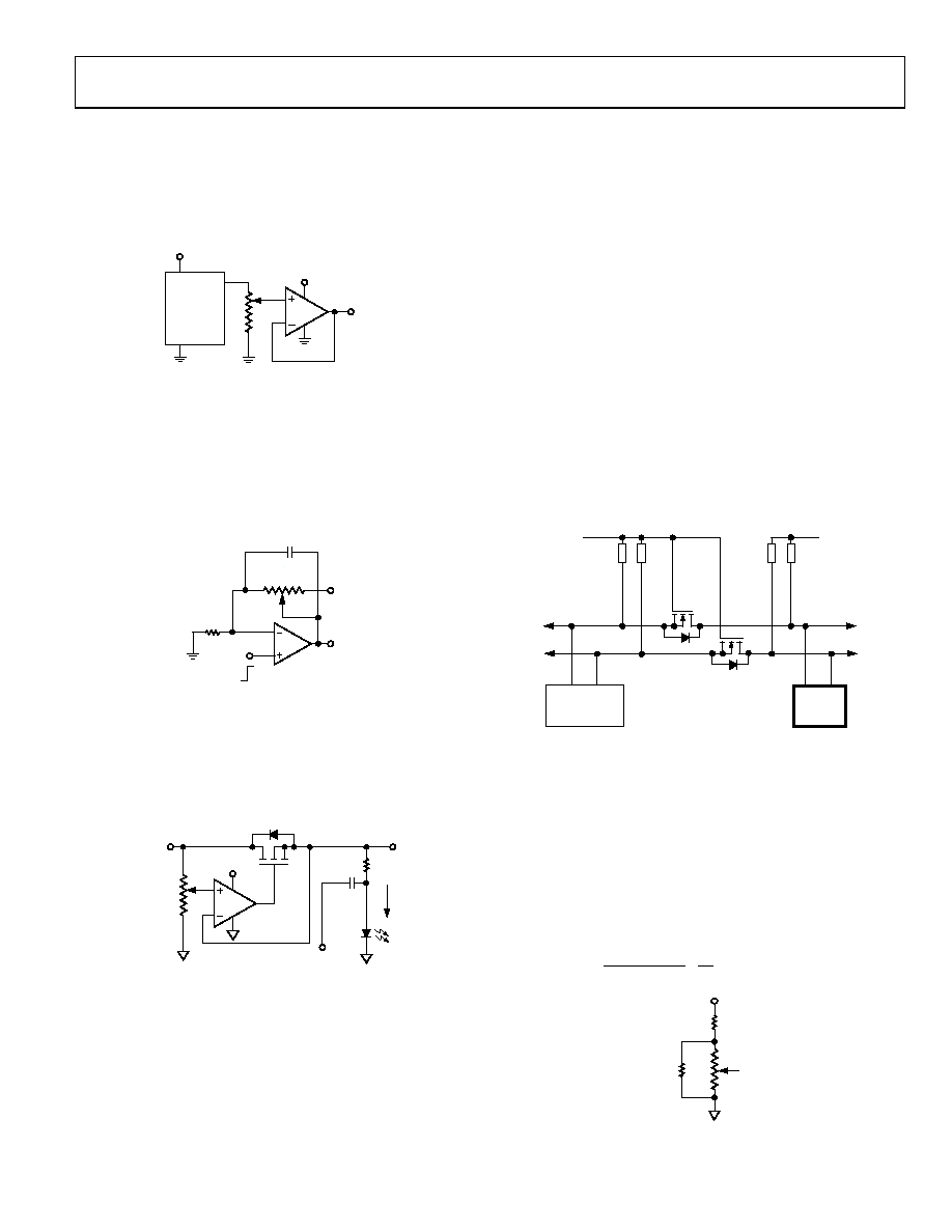
LEVEL SHIFTING FOR DIFFERENT VOLTAGE
OPERATION
If the SCL and SDA signals come from a low voltage logic
controller and are below the minimum VIH level (0.7 V × VDD),
level shift the signals for read/write communications between
the AD5171 and the controller. Figure 42 shows one of the
implementations. For example, when SDA1 is at 2.5 V, M1 turns
off, and SDA2 becomes 5 V. When SDA1 is at 0 V, M1 turns on,
and SDA2 approaches 0 V. As a result, proper level shifting is
established. M1 and M2 should be low threshold N-Ch power
MOSFETs, such as FDV301N.
2.5V
CONTROLLER
2.7V–5.5V
AD5171
Rp
VDD1 = 2.5V
VDD2 = 5V
G
S
D
M1
S
D
M2
SDA1
SCL1
SDA2
SCL2
03
43
7-
0
42
Figure 42. Level Shifting for Different Voltage Operation
RESISTANCE SCALING
The AD5171 offers 5 kΩ, 10 kΩ, 50 kΩ, and 100 kΩ nominal
resistances. For users who need to optimize the resolution with
an arbitrary full range resistance, the following techniques can
be used. By paralleling a discrete resistor, a proportionately lower
voltage appears at Terminal A to Terminal B, which is applicable
only to the voltage divider mode (see Figure 43).
This translates into a finer degree of precision because the step
size at Terminal W is smaller. The voltage can be found as
DD
AB
W
V
D
R2
R
R3
R2
R
D
V
×
+
=
64
||
)
||
(
)
(
(5)
R1
R2
B
A
VDD
R3
W
03
43
7-
04
3
Figure 43. Lowering the Nominal Resistance
相关PDF资料 |
PDF描述 |
|---|---|
| AD5171BRJZ50-R7 | IC DGTL POT OTP 50K SOT23-8 |
| MS3108A28-3P | CONN PLUG 3POS RT ANG W/PINS |
| AD5171BRJZ100-R7 | IC DGTL POT OTP 100K SOT23-8 |
| DS1386P-32-120+ | IC TIMEKEEPER RAM 256K 32-PCM |
| AD5171BRJZ10-R7 | IC DGTL POT OTP 10K SOT23-8 |
相关代理商/技术参数 |
参数描述 |
|---|---|
| AD5171EVAL | 功能描述:BOARD EVAL FOR AD5171 RoHS:否 类别:编程器,开发系统 >> 评估演示板和套件 系列:- 产品培训模块:Obsolescence Mitigation Program 标准包装:1 系列:- 主要目的:电源管理,电池充电器 嵌入式:否 已用 IC / 零件:MAX8903A 主要属性:1 芯锂离子电池 次要属性:状态 LED 已供物品:板 |
| AD5172 | 制造商:AD 制造商全称:Analog Devices 功能描述:256-Position One-Time Programmable Dual-Channel I2C Digital Potentiometers |
| AD5172BRM10 | 功能描述:IC POT DUAL 10K 256POS 10-MSOP RoHS:否 类别:集成电路 (IC) >> 数据采集 - 数字电位器 系列:- 标准包装:3,000 系列:DPP 接片:32 电阻(欧姆):10k 电路数:1 温度系数:标准值 300 ppm/°C 存储器类型:非易失 接口:3 线串行(芯片选择,递增,增/减) 电源电压:2.5 V ~ 6 V 工作温度:-40°C ~ 85°C 安装类型:表面贴装 封装/外壳:8-WFDFN 裸露焊盘 供应商设备封装:8-TDFN(2x3) 包装:带卷 (TR) |
| AD5172BRM100 | 功能描述:IC POT DUAL 100K 256POS 10-MSOP RoHS:否 类别:集成电路 (IC) >> 数据采集 - 数字电位器 系列:- 标准包装:3,000 系列:DPP 接片:32 电阻(欧姆):10k 电路数:1 温度系数:标准值 300 ppm/°C 存储器类型:非易失 接口:3 线串行(芯片选择,递增,增/减) 电源电压:2.5 V ~ 6 V 工作温度:-40°C ~ 85°C 安装类型:表面贴装 封装/外壳:8-WFDFN 裸露焊盘 供应商设备封装:8-TDFN(2x3) 包装:带卷 (TR) |
| AD5172BRM100-RL7 | 制造商:Analog Devices 功能描述:Digital Potentiometer 256POS 100KOhm Dual 10-Pin MSOP T/R 制造商:Analog Devices 功能描述:DGTL POTENTIOMETER 256POS 100KOHM DUAL 10MSOP - Tape and Reel |
发布紧急采购,3分钟左右您将得到回复。