参数资料
| 型号: | AD5201BRMZ50 |
| 厂商: | Analog Devices Inc |
| 文件页数: | 11/15页 |
| 文件大小: | 0K |
| 描述: | IC DGTL POT 50K 33POS 10-MSOP |
| 标准包装: | 50 |
| 接片: | 33 |
| 电阻(欧姆): | 50k |
| 电路数: | 1 |
| 温度系数: | 标准值 500 ppm/°C |
| 存储器类型: | 易失 |
| 接口: | 3 线串行(芯片选择) |
| 电源电压: | 2.7 V ~ 5.5 V,±2.3 V ~ 2.7 V |
| 工作温度: | -40°C ~ 85°C |
| 安装类型: | 表面贴装 |
| 封装/外壳: | 10-TFSOP,10-MSOP(0.118",3.00mm 宽) |
| 供应商设备封装: | 10-MSOP |
| 包装: | 管件 |
AD5200/AD5201
–5–
ABSOLUTE MAXIMUM RATINGS
1
(TA = 25
°C, unless otherwise noted)
VDD to VSS . . . . . . . . . . . . . . . . . . . . . . . . . . . . . . . . . . . . . 7 V
VDD to GND . . . . . . . . . . . . . . . . . . . . . . . . . . . . . –0.3, +7 V
VSS to GND . . . . . . . . . . . . . . . . . . . . . . . . . . . . . . . 0 V, –7 V
VA, VB, VW to GND . . . . . . . . . . . . . . . . . . . . . . . . . VSS, VDD
IMAX . . . . . . . . . . . . . . . . . . . . . . . . . . . . . . . . . . . . .
±20 mA2
Digital Inputs and Output Voltage to GND . . . . . . . 0 V, 7 V
Operating Temperature Range . . . . . . . . . . . –40
°C to +85°C
Maximum Junction Temperature (TJ Max) . . . . . . . . . 150
°C
Storage Temperature . . . . . . . . . . . . . . . . . . –65
°C to +150°C
Lead Temperature (Soldering, 10 sec) . . . . . . . . . . . . 300
°C
Thermal Resistance
θ
JA,
. . . . . . . . . . . . . 200
°C/W
Package Power Dissipation = (TJ Max – TA)/
θJA
NOTES
1Stresses above those listed under Absolute Maximum Ratings may cause perma-
nent damage to the device. This is a stress rating; functional operation of the device
at these or any other conditions above those listed in the operational sections of this
specification is not implied. Exposure to absolute maximum rating conditions for
extended periods may affect device reliability.
2Max current is bounded by the maximum current handling of the switches,
maximum power dissipation of the package, and maximum applied voltage across
any two of the A, B, and W terminals at a given resistance. Please refer to TPC 31
and TPC 32 for detail.
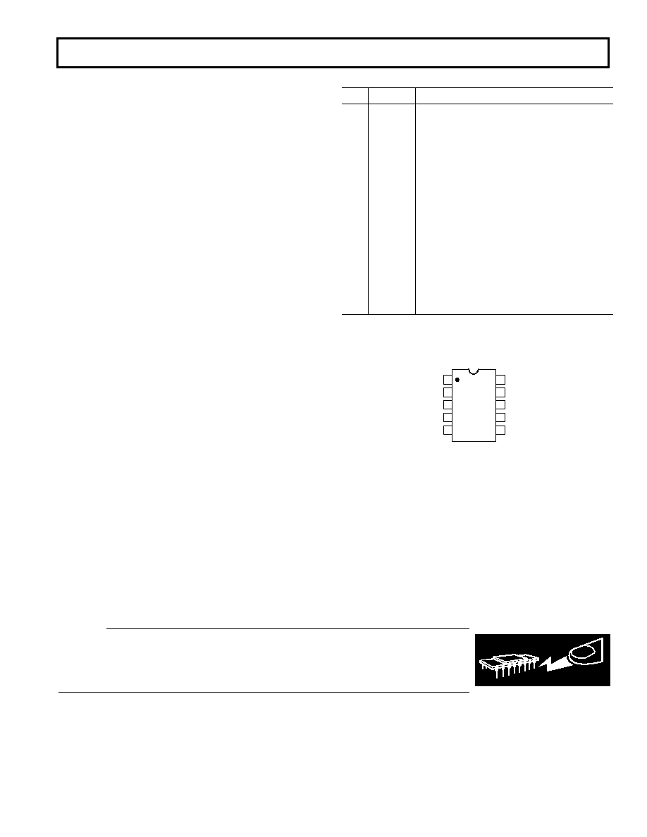
PIN CONFIGURATION
TOP VIEW
(Not to Scale)
10
9
8
7
6
1
2
3
4
5
AD5200/
AD5201
B
VSS
GND
CS
SDI
A
W
VDD
SHDN
CLK
CAUTION
ESD (electrostatic discharge) sensitive device. Electrostatic charges as high as 4000 V readily
accumulate on the human body and test equipment and can discharge without detection. Although
the AD5200/AD5201 features proprietary ESD protection circuitry, permanent damage may occur
on devices subjected to high-energy electrostatic discharges. Therefore, proper ESD precautions
are recommended to avoid performance degradation or loss of functionality.
WARNING!
ESD SENSITIVE DEVICE
PIN FUNCTION DESCRIPTIONS
Pin
Name
Description
1
B
B Terminal.
2VSS
Negative Power Supply, specified for opera-
tion from 0 V to –2.7 V.
3
GND
Ground.
4
CS
Chip Select Input, Active Low. When
CS
returns high, data will be loaded into the
DAC register.
5
SDI
Serial Data Input.
6
CLK
Serial Clock Input, positive edge triggered.
7
SHDN
Active Low Input. Terminal A open circuit.
Shutdown controls Variable Resistors of
RDAC to temporary infinite.
8VDD
Positive Power Supply (Sum of VDD + VSS
≤ 5.5 V).
9
W
Wiper Terminal.
10
A
A Terminal.
MSOP
REV. D
相关PDF资料 |
PDF描述 |
|---|---|
| MS27472P16B6P | CONN RCPT 6POS WALL MT W/PINS |
| VI-J0V-MZ | CONVERTER MOD DC/DC 5.8V 25W |
| MS27484T14F97PB | CONN PLUG 12POS STRAIGHT W/PINS |
| VI-J1Z-MZ | CONVERTER MOD DC/DC 2V 10W |
| MS3106E32-1P | CONN PLUG 5POS STRAIGHT W/PINS |
相关代理商/技术参数 |
参数描述 |
|---|---|
| AD5201BRMZ50-REEL7 | 功能描述:IC DGTL POT 50K 33POS 10-MSOP RoHS:是 类别:集成电路 (IC) >> 数据采集 - 数字电位器 系列:- 标准包装:3,000 系列:DPP 接片:32 电阻(欧姆):10k 电路数:1 温度系数:标准值 300 ppm/°C 存储器类型:非易失 接口:3 线串行(芯片选择,递增,增/减) 电源电压:2.5 V ~ 6 V 工作温度:-40°C ~ 85°C 安装类型:表面贴装 封装/外壳:8-WFDFN 裸露焊盘 供应商设备封装:8-TDFN(2x3) 包装:带卷 (TR) |
| AD5201TD | 制造商:未知厂家 制造商全称:未知厂家 功能描述:Analog-to-Digital Converter, 12-Bit |
| AD5201TD/883B | 制造商:未知厂家 制造商全称:未知厂家 功能描述:Analog-to-Digital Converter, 12-Bit |
| AD5202BD | 制造商:未知厂家 制造商全称:未知厂家 功能描述:Analog-to-Digital Converter, 12-Bit |
| AD5202TD | 制造商:未知厂家 制造商全称:未知厂家 功能描述:Analog-to-Digital Converter, 12-Bit |
发布紧急采购,3分钟左右您将得到回复。