- 您现在的位置:买卖IC网 > PDF目录9303 > AD5207BRU10-REEL7 (Analog Devices Inc)IC DGTL POT DUAL 256POS 14TSSOP PDF资料下载
参数资料
| 型号: | AD5207BRU10-REEL7 |
| 厂商: | Analog Devices Inc |
| 文件页数: | 16/16页 |
| 文件大小: | 0K |
| 描述: | IC DGTL POT DUAL 256POS 14TSSOP |
| 标准包装: | 1,000 |
| 接片: | 256 |
| 电阻(欧姆): | 10k |
| 电路数: | 2 |
| 温度系数: | 标准值 500 ppm/°C |
| 存储器类型: | 易失 |
| 接口: | 4 线 SPI(芯片选择) |
| 电源电压: | 2.7 V ~ 5.5 V,±2.2 V ~ 2.7 V |
| 工作温度: | -40°C ~ 125°C |
| 安装类型: | 表面贴装 |
| 封装/外壳: | 14-TSSOP(0.173",4.40mm 宽) |
| 供应商设备封装: | 14-TSSOP |
| 包装: | 带卷 (TR) |
REV. 0
AD5207
–9–
OPERATION
The AD5207 provides a dual channel, 256-position digitally
controlled variable resistor (VR) device. The terms VR, RDAC,
and digital potentiometer are sometimes used interchangeably.
Changing the programmable VR settings is accomplished by
clocking in a 10-bit serial data word into the SDI (Serial Data
Input) pin. The format of this data word is two address Bits, A1
and A0. With A1 and A2 are first and second bits respectively,
followed by eight data bits B7–B0 with MSB first. Table I pro-
vides the serial register data word format. See Table III for the
AD5207 address assignments to decode the location of VR latch
receiving the serial register data in Bits B7 through B0. VR settings
can be changed one at a time in random sequence. The AD5207
presets to a midscale during power-on condition. AD5207 contains
a power shutdown
SHDN pin. When activated in logic low.
Terminals A on both RDACs will be open-circuited while the
wiper terminals WX are shorted to BX. As a result, a minimum
amount of leakage current will be consumed in both RDACs,
and the power dissipation is negligible. During the shutdown
mode, the VR latch settings are maintained. Thus the previ-
ous resistance values remain when the devices are resumed
from the shutdown.
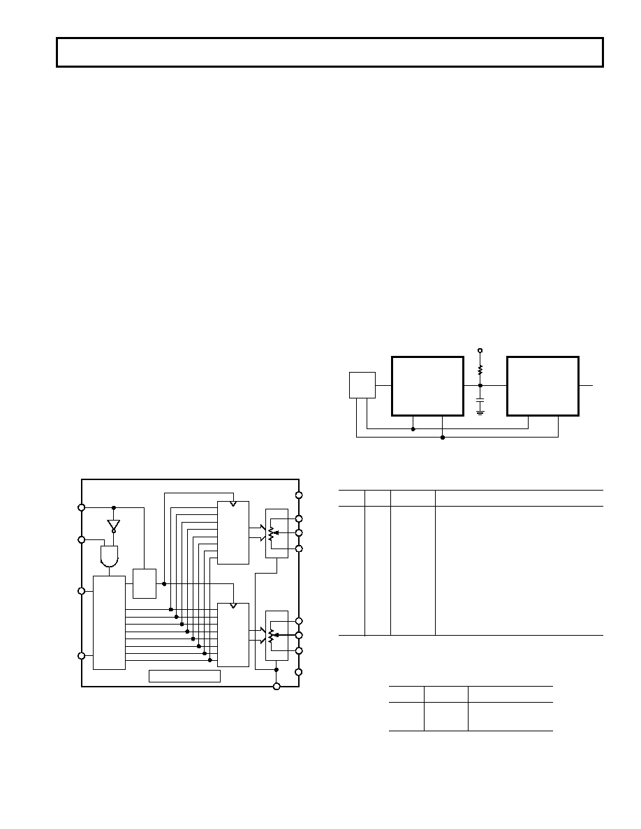
DIGITAL INTERFACING
The AD5207 contains a standard three-wire serial input control
interface. The three inputs are clock (CLK), chip select (
CS),
and serial data input (SDI). The positive edge-sensitive CLK
input requires clean transitions to avoid clocking incorrect data
into the serial input register. Standard logic families work well.
If mechanical switches are used for product evaluation, they
should be debounced by a flip-flop or other suitable means. Fig-
ure 2 shows more detail of the internal digital circuitry. When
CS
is low, the clock loads data into the serial register on each posi-
tive clock edge; see Table II.
SER
REG
A0
D7
D6
D5
D4
D3
D2
D1
D0
ADDR
DEC
EN
RDAC
LATCH
#2
RDAC
LATCH
#1
AD5207
POWER-ON RESET
SHDN
VDD
A1
W1
B1
A2
W2
B2
VSS
CS
CLK
SDO
SDI
Figure 2. Block Diagram
The serial-data-output (SDO) pin contains an open drain
n-channel FET. This output requires a pull-up resistor in order
to transfer data to the next package’s SDI pin. The pull-up
resistor termination voltage may be larger than the VDD supply
of the AD5207 SDO output device, e.g., the AD5207 could
operate at VDD = 3.3 V and the pull-up for interface to the next
device could be set at 5 V. This allows for daisy chaining several
RDACs from a single processor serial-data line. The clock period
may need to be increased when using a pull-up resistor to the
SDI pin of the following devices in series. Capacitive loading at
the daisy chain node SDO–SDI between devices may add time
delay to subsequent devices. User should be aware of this poten-
tial problem in order to successfully achieve data transfer. See
Figure 3. When configuring devices for daisy-chaining, the
CS
should be kept low until all the bits of every package are clocked
into their respective serial registers, ensuring that the address bit
and data bits are in the proper decoding location. This requires
20 bits of address and data complying with the data word in
Table I if two AD5207 RDACs are daisy chained. During shut-
down
SHDN, the SDO output pin is forced to OFF (logic high
state) to disable power dissipation in the pull-up resistor. See
Figure 4 for equivalent SDO output circuit schematic.
RP
2k
AD5207
SDO
SDI
CLK
CS
AD5207
SDO
SDI
CLK
CS
C
+V
Figure 3. Daisy-Chain Configuration Using SDO
Table II. Input Logic Control Truth Table
CLK
CS
SHDN
Register Activity
L
H
No SR effect, enables SDO pin.
P
L
H
Shift one bit in from the SDI pin. MSB
first. The tenth previously entered bit
is shifted out of the SDO pin.
X
P
H
Load SR data into RDAC latch based
on A0 decode (Table III).
X
H
No Operation.
X
H
L
Open circuits all resistor A Terminals,
connects W to B, turns off SDO out-
put transistor.
NOTE
P = positive edge, X = don’t care, SR = shift register.
Table III. Address Decode Table
A1
A0
Latch Loaded
0
RDAC #1
0
1
RDAC #2
相关PDF资料 |
PDF描述 |
|---|---|
| MS27467T21B11PD | CONN PLUG 11POS STRAIGHT W/PINS |
| DS1100Z-125+ | IC DELAY LINE 5TAP 125NS 8-SOIC |
| VE-2NF-MY-F3 | CONVERTER MOD DC/DC 72V 50W |
| AD5248BRM50-RL7 | IC DGTL POT DUAL 50K I2C 10-MSOP |
| DS1100Z-30+ | IC DELAY LINE 5TAP 30NS 8-SOIC |
相关代理商/技术参数 |
参数描述 |
|---|---|
| AD5207BRU50 | 功能描述:IC DGTL POT DUAL 256POS 14TSSOP RoHS:否 类别:集成电路 (IC) >> 数据采集 - 数字电位器 系列:- 标准包装:3,000 系列:DPP 接片:32 电阻(欧姆):10k 电路数:1 温度系数:标准值 300 ppm/°C 存储器类型:非易失 接口:3 线串行(芯片选择,递增,增/减) 电源电压:2.5 V ~ 6 V 工作温度:-40°C ~ 85°C 安装类型:表面贴装 封装/外壳:8-WFDFN 裸露焊盘 供应商设备封装:8-TDFN(2x3) 包装:带卷 (TR) |
| AD5207BRU50-REEL7 | 功能描述:IC DGTL POT DUAL 256POS 14TSSOP RoHS:否 类别:集成电路 (IC) >> 数据采集 - 数字电位器 系列:- 标准包装:3,000 系列:DPP 接片:32 电阻(欧姆):10k 电路数:1 温度系数:标准值 300 ppm/°C 存储器类型:非易失 接口:3 线串行(芯片选择,递增,增/减) 电源电压:2.5 V ~ 6 V 工作温度:-40°C ~ 85°C 安装类型:表面贴装 封装/外壳:8-WFDFN 裸露焊盘 供应商设备封装:8-TDFN(2x3) 包装:带卷 (TR) |
| AD5207BRUZ10 | 功能描述:IC DGTL POT DUAL 10K 14-TSSOP RoHS:是 类别:集成电路 (IC) >> 数据采集 - 数字电位器 系列:- 产品培训模块:Lead (SnPb) Finish for COTS Obsolescence Mitigation Program 标准包装:1 系列:- 接片:256 电阻(欧姆):100k 电路数:1 温度系数:标准值 35 ppm/°C 存储器类型:非易失 接口:3 线串口 电源电压:2.7 V ~ 5.25 V 工作温度:-40°C ~ 85°C 安装类型:表面贴装 封装/外壳:8-WDFN 裸露焊盘 供应商设备封装:8-TDFN-EP(3x3) 包装:剪切带 (CT) 产品目录页面:1399 (CN2011-ZH PDF) 其它名称:MAX5423ETA+TCT |
| AD5207BRUZ100 | 功能描述:IC DGTL POT DUAL 256POS 14-TSSOP RoHS:是 类别:集成电路 (IC) >> 数据采集 - 数字电位器 系列:- 产品培训模块:Lead (SnPb) Finish for COTS Obsolescence Mitigation Program 标准包装:1 系列:- 接片:256 电阻(欧姆):100k 电路数:1 温度系数:标准值 35 ppm/°C 存储器类型:非易失 接口:3 线串口 电源电压:2.7 V ~ 5.25 V 工作温度:-40°C ~ 85°C 安装类型:表面贴装 封装/外壳:8-WDFN 裸露焊盘 供应商设备封装:8-TDFN-EP(3x3) 包装:剪切带 (CT) 产品目录页面:1399 (CN2011-ZH PDF) 其它名称:MAX5423ETA+TCT |
| AD5207BRUZ100-R7 | 功能描述:IC POT DGTL DUAL 256POS 14TSSOP RoHS:是 类别:集成电路 (IC) >> 数据采集 - 数字电位器 系列:- 标准包装:3,000 系列:DPP 接片:32 电阻(欧姆):10k 电路数:1 温度系数:标准值 300 ppm/°C 存储器类型:非易失 接口:3 线串行(芯片选择,递增,增/减) 电源电压:2.5 V ~ 6 V 工作温度:-40°C ~ 85°C 安装类型:表面贴装 封装/外壳:8-WFDFN 裸露焊盘 供应商设备封装:8-TDFN(2x3) 包装:带卷 (TR) |
发布紧急采购,3分钟左右您将得到回复。