- 您现在的位置:买卖IC网 > PDF目录9430 > AD5207BRUZ100 (Analog Devices Inc)IC DGTL POT DUAL 256POS 14-TSSOP PDF资料下载
参数资料
| 型号: | AD5207BRUZ100 |
| 厂商: | Analog Devices Inc |
| 文件页数: | 3/16页 |
| 文件大小: | 0K |
| 描述: | IC DGTL POT DUAL 256POS 14-TSSOP |
| 标准包装: | 96 |
| 接片: | 256 |
| 电阻(欧姆): | 100k |
| 电路数: | 2 |
| 温度系数: | 标准值 500 ppm/°C |
| 存储器类型: | 易失 |
| 接口: | 4 线 SPI(芯片选择) |
| 电源电压: | 2.7 V ~ 5.5 V,±2.2 V ~ 2.7 V |
| 工作温度: | -40°C ~ 125°C |
| 安装类型: | 表面贴装 |
| 封装/外壳: | 14-TSSOP(0.173",4.40mm 宽) |
| 供应商设备封装: | 14-TSSOP |
| 包装: | 管件 |
| 产品目录页面: | 786 (CN2011-ZH PDF) |
REV. 0
AD5207
–11–
Table IV.
DRWB
(DEC)
( )
Output State
255
10006
Full-Scale (RAB – 1 LSB + RW)
128
5045
Midscale
184
1 LSB
0
45
Zero-Scale (Wiper Contact Resistance)
Note that in the zero-scale condition a finite wiper resistance of
45
is present. Care should be taken to limit the current flow
between W and B in this state to a maximum current of no more
than 5 mA. Otherwise, degradation or possibly destruction of
the internal switch contacts can occur.
Similar to the mechanical potentiometer, the resistance of the
RDAC between the wiper W and Terminal A also produces a
digitally controlled resistance RWA. When these terminals are used,
the B Terminal should be let open or tied to the wiper terminal.
Setting the resistance value for RWA starts at a maximum value
of resistance and decreases as the data loaded in the latch is
increased in value. The general equation for this operation is:
RD
D
RR
WA
AB
W
() =×
+
256
–
(2)
For example, when RAB = 10 k
, B terminal is either open or
tied to W, the following output resistance, RWA, will be set for
the following RDAC latch codes.
Table V.
DRWA
(DEC)
( )
Output State
255
84
Full-Scale (RAB/256 + RW)
128
5045
Midscale
1
10006
1 LSB
0
10045
Zero-Scale
The typical distribution of RAB from channel to channel matches
within
±1%. Device-to-device matching is process-lot depen-
dent and is possible to have
±30% variation. The change in RAB
with temperature has a 500 ppm/
°C temperature coefficient.
PROGRAMMING THE POTENTIOMETER DIVIDER
Voltage Output Operation
The digital potentiometer easily generates an output voltage
proportional to the input voltage. Let’s ignore the effect of
the wiper resistance for the moment. For example, when con-
necting A Terminal to 5 V and B Terminal to ground, it produces
a programmable output voltage at the wiper starting at zero
volts up to 1 LSB less than 5 V. Each LSB of voltage is equal
to the voltage applied across terminal AB divided by the 256
position of the potentiometer divider. Since AD5207 is capable
for dual supplies, the general equation defining the output volt-
age with respect to ground for any given input voltage applied to
terminals AB is:
VD
D
V
D
V
WA
B
() =+
256
(3)
Operation of the digital potentiometer in the divider mode
results in more accurate operation over temperature. Unlike the
rheostat mode, the output voltage is dependent on the ratio of
RWA and RWB and not the absolute values; therefore, the drift
reduces to 15 ppm/
°C. There is no voltage polarity constraint
between Terminals A, B, and W as long as the terminal voltage
stays within VSS < VTERM < VDD.
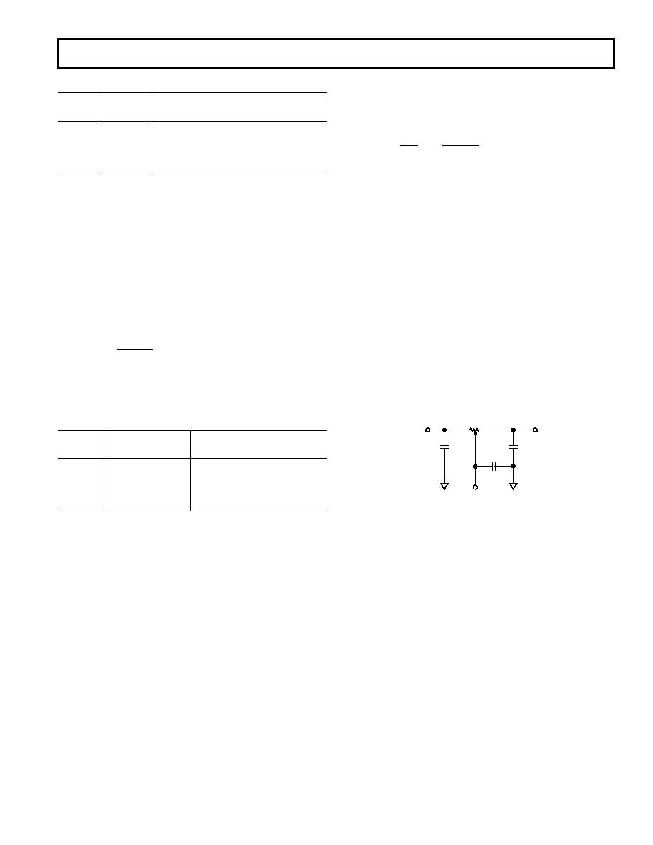
RDAC CIRCUIT SIMULATION MODEL
The internal parasitic capacitances and the external capacitive
loads dominate the ac characteristics of the RDACs. Config-
ured as a potentiometer divider the –3 dB bandwidth of the
AD5207BRU10 (10 k
resistor) measures 600 kHz at half
scale. TPC 16 provides the large signal BODE plot characteris-
tics of the three available resistor versions 10 k
and 50 k.
The gain flatness versus frequency graph, TPC 16, predicts
filter applications performance. A parasitic simulation model has
been developed and is shown in Figure 9. Listing I provides a
macro model net list for the 10 k
RDAC:
CW
70pF
CB
CA
B
A
RDAC
10k
W
CB = 45pF
CA = 45pF
Figure 9. RDAC Circuit Simulation Model for RDAC = 10 k
Listing I. Macro Model Net List for RDAC
.PARAM D=255, RDAC=10E3
*
.SUBCKT DPOT (A,W)
*
CA A 0 45E-12
RAW A W {(1-D/256)
*RDAC+50}
CW W 0 70E-12
RBW W B {D/256
*RDAC+50}
CB B 0 45E-12
*
.ENDS DPOT
相关PDF资料 |
PDF描述 |
|---|---|
| AD5241BRUZ10-R7 | IC DGTL POT 256POS 10K 14TSSOP |
| AD5241BRZ10 | IC POT DGTL SGL 256POS 14-SOIC |
| VE-23R-MY-F2 | CONVERTER MOD DC/DC 7.5V 50W |
| VE-23R-MY-F1 | CONVERTER MOD DC/DC 7.5V 50W |
| VI-B3H-IU-F2 | CONVERTER MOD DC/DC 52V 200W |
相关代理商/技术参数 |
参数描述 |
|---|---|
| AD5207BRUZ100-R7 | 功能描述:IC POT DGTL DUAL 256POS 14TSSOP RoHS:是 类别:集成电路 (IC) >> 数据采集 - 数字电位器 系列:- 标准包装:3,000 系列:DPP 接片:32 电阻(欧姆):10k 电路数:1 温度系数:标准值 300 ppm/°C 存储器类型:非易失 接口:3 线串行(芯片选择,递增,增/减) 电源电压:2.5 V ~ 6 V 工作温度:-40°C ~ 85°C 安装类型:表面贴装 封装/外壳:8-WFDFN 裸露焊盘 供应商设备封装:8-TDFN(2x3) 包装:带卷 (TR) |
| AD5207BRUZ10-RL7 | 功能描述:IC DGTL POT DUAL 10K 14-TSSOP RoHS:是 类别:集成电路 (IC) >> 数据采集 - 数字电位器 系列:- 标准包装:3,000 系列:DPP 接片:32 电阻(欧姆):10k 电路数:1 温度系数:标准值 300 ppm/°C 存储器类型:非易失 接口:3 线串行(芯片选择,递增,增/减) 电源电压:2.5 V ~ 6 V 工作温度:-40°C ~ 85°C 安装类型:表面贴装 封装/外壳:8-WFDFN 裸露焊盘 供应商设备封装:8-TDFN(2x3) 包装:带卷 (TR) |
| AD5207BRUZ50 | 功能描述:IC DGTL POT 256POS 50K 14TSSOP RoHS:是 类别:集成电路 (IC) >> 数据采集 - 数字电位器 系列:- 产品培训模块:Lead (SnPb) Finish for COTS Obsolescence Mitigation Program 标准包装:1 系列:- 接片:256 电阻(欧姆):100k 电路数:1 温度系数:标准值 35 ppm/°C 存储器类型:非易失 接口:3 线串口 电源电压:2.7 V ~ 5.25 V 工作温度:-40°C ~ 85°C 安装类型:表面贴装 封装/外壳:8-WDFN 裸露焊盘 供应商设备封装:8-TDFN-EP(3x3) 包装:剪切带 (CT) 产品目录页面:1399 (CN2011-ZH PDF) 其它名称:MAX5423ETA+TCT |
| AD5207BRUZ50-RL7 | 功能描述:IC DGTL POT DUAL 50K 14-TSSOP RoHS:是 类别:集成电路 (IC) >> 数据采集 - 数字电位器 系列:- 标准包装:3,000 系列:DPP 接片:32 电阻(欧姆):10k 电路数:1 温度系数:标准值 300 ppm/°C 存储器类型:非易失 接口:3 线串行(芯片选择,递增,增/减) 电源电压:2.5 V ~ 6 V 工作温度:-40°C ~ 85°C 安装类型:表面贴装 封装/外壳:8-WFDFN 裸露焊盘 供应商设备封装:8-TDFN(2x3) 包装:带卷 (TR) |
| AD521 | 制造商:AD 制造商全称:Analog Devices 功能描述:Integrated Circuit Precision Instrumentation Amplifier |
发布紧急采购,3分钟左右您将得到回复。