参数资料
| 型号: | AD5207BRUZ50 |
| 厂商: | Analog Devices Inc |
| 文件页数: | 2/16页 |
| 文件大小: | 0K |
| 描述: | IC DGTL POT 256POS 50K 14TSSOP |
| 标准包装: | 96 |
| 接片: | 256 |
| 电阻(欧姆): | 50k |
| 电路数: | 2 |
| 温度系数: | 标准值 500 ppm/°C |
| 存储器类型: | 易失 |
| 接口: | 4 线 SPI(芯片选择) |
| 电源电压: | 2.7 V ~ 5.5 V,±2.2 V ~ 2.7 V |
| 工作温度: | -40°C ~ 125°C |
| 安装类型: | 表面贴装 |
| 封装/外壳: | 14-TSSOP(0.173",4.40mm 宽) |
| 供应商设备封装: | 14-TSSOP |
| 包装: | 管件 |
REV. 0
AD5207
–10–
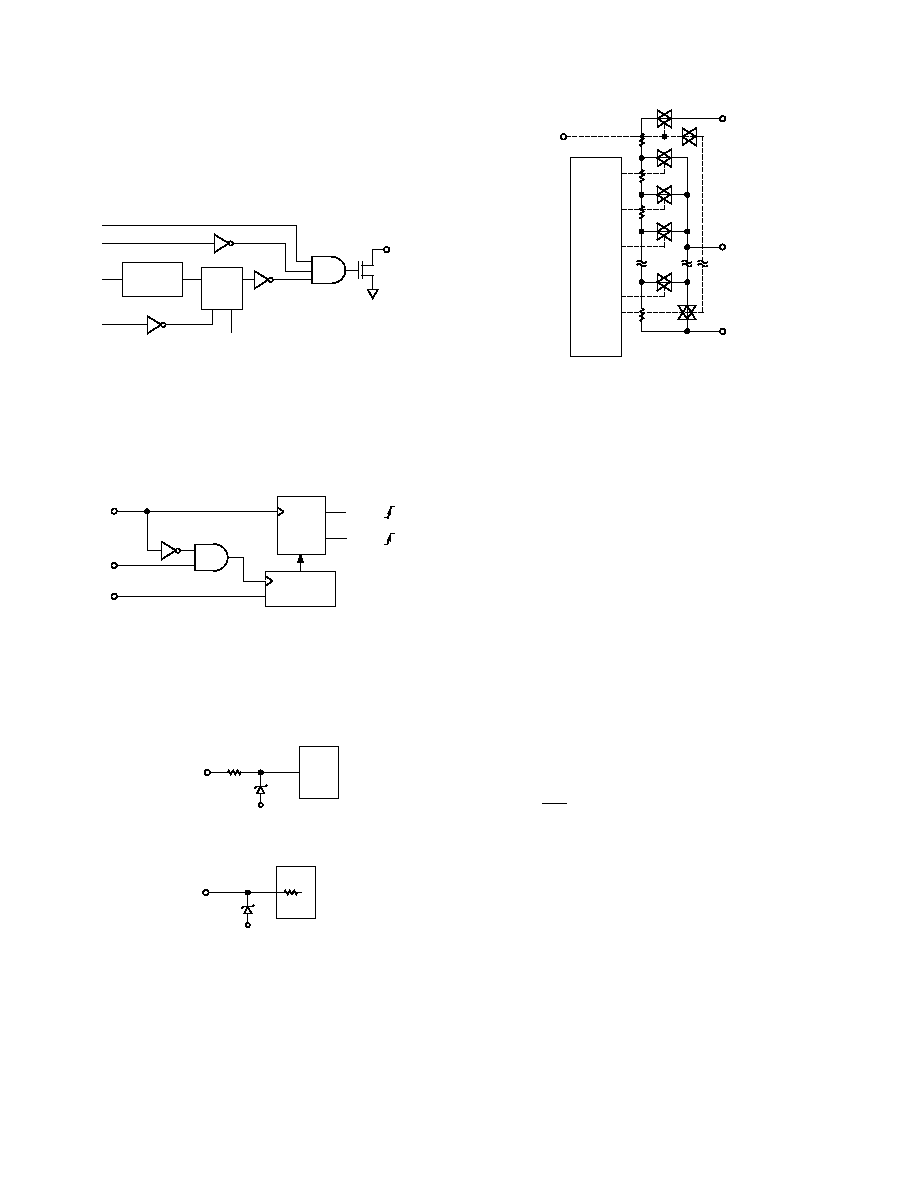
The data setup and data hold times in the specification table
determine the data valid time requirements. The last ten bits of
the data word entered into the serial register are held when
CS
returns high and any extra bits are ignored. At the same time, when
CS goes high, it gates the address decoder enabling one of two
positive edge-triggered AD5207 RDAC latches; see Figure 5 detail.
SDI
CLK
CS
CK RS
D
Q
SERIAL
REGISTER
SDO
SHDN
INTERNAL
RS
Figure 4. Detail SDO Output Schematic of the AD5207
The target RDAC latch is loaded with the last eight bits of the
data word to complete one RDAC update. For AD5207, it
cannot update both channels simultaneously and therefore, two
separate 10-bit data words must be clocked in to change both
VR settings.
RDAC1
RDAC2
ADDR
DECODE
SERIAL
REGISTER
AD5207
SDI
CLK
CS
Figure 5. Equivalent Input Control Logic
All digital inputs are protected with a series input resistor and
parallel Zener ESD structure shown in Figures 6 and 7. Applies
to digital input pins
CS, SDI, SDO, SHDN, and CLK. Digital
input level for Logic 1 can be anywhere from 2.4 V to 5 V
regardless of whether it is in single or dual supplies.
340
VSS
LOGIC
DIGITAL PIN
Figure 6. ESD Protection of Digital Pins
A,B,W
VSS
Figure 7. ESD Protection of Resistor Terminals
D7
D6
D5
D4
D3
D2
D1
D0
RDAC
LATCH
AND
DECODER
RS
SHDN
Ax
Wx
Bx
Figure 8. Equivalent RDAC Circuit
PROGRAMMING THE VARIABLE RESISTOR
Rheostat Operation
The nominal resistance of the RDAC between Terminals A and
B is available with values of 10 k
, 50 k, and 100 k. The last
few digits of the part number determine the nominal resistance
value, e.g., 10 k
= 10; 50 k = 50; and 100 k = 100. The
nominal resistance (RAB) of the VR has 256 contact points
accessed by the wiper terminal, plus the B Terminal contact.
The 8-bit data in the RDAC latch is decoded to select one of
the 256 possible settings. Assume a 10 k
part is used, the
wiper’s first connection starts at the B Terminal for data 00H.
Since there is a 45
wiper contact resistance, such connection
yields a minimum of 45
resistance between Terminals W and
B. The second connection is the first tap point corresponds to
84
(R
WB = RAB/256 + RW = 39
+ 45 ) for data 01
H. The
third connection is the next tap point representing 123
(39 ×
2 + 45) for data 02H and so on. Each LSB value increase moves
the wiper up the resistor ladder until the last tap point is reached at
10006
(RAB – 1 LSB + RW). Figure 8 shows a simplified dia-
gram of the equivalent RDAC circuit.
The general equation determining the programmable output
resistance between W and B is:
RD
D
RR
WB
AB
W
() =×
+
256
(1)
where D is the data contained in the 8-bit RDAC latch, and RAB
is the nominal end-to-end resistance.
For example, RAB =10 k
, A Terminal can be open-circuit or
tied to W. The following output resistance RWB will be set for
the following RDAC latch codes.
相关PDF资料 |
PDF描述 |
|---|---|
| AD5207BRUZ10 | IC DGTL POT DUAL 10K 14-TSSOP |
| AD5207BRUZ100 | IC DGTL POT DUAL 256POS 14-TSSOP |
| AD5241BRUZ10-R7 | IC DGTL POT 256POS 10K 14TSSOP |
| AD5241BRZ10 | IC POT DGTL SGL 256POS 14-SOIC |
| VE-23R-MY-F2 | CONVERTER MOD DC/DC 7.5V 50W |
相关代理商/技术参数 |
参数描述 |
|---|---|
| AD5207BRUZ50-RL7 | 功能描述:IC DGTL POT DUAL 50K 14-TSSOP RoHS:是 类别:集成电路 (IC) >> 数据采集 - 数字电位器 系列:- 标准包装:3,000 系列:DPP 接片:32 电阻(欧姆):10k 电路数:1 温度系数:标准值 300 ppm/°C 存储器类型:非易失 接口:3 线串行(芯片选择,递增,增/减) 电源电压:2.5 V ~ 6 V 工作温度:-40°C ~ 85°C 安装类型:表面贴装 封装/外壳:8-WFDFN 裸露焊盘 供应商设备封装:8-TDFN(2x3) 包装:带卷 (TR) |
| AD521 | 制造商:AD 制造商全称:Analog Devices 功能描述:Integrated Circuit Precision Instrumentation Amplifier |
| AD521-.2 | 制造商:Assmann Electronics Inc 功能描述: |
| AD5210 | 制造商:AD 制造商全称:Analog Devices 功能描述:12 BIT SUCCESSIVE APPROXIMATION HIGH ACCURACY A/D CONVERTERS |
| AD521-00E | 功能描述:SENSOR MAG SW 20G CROS AX 8-MSOP 制造商:nve corp/sensor products 系列:AD 包装:管件 零件状态:有效 功能:全极开关 技术:霍尔效应 极化:任意一种 感应范围:±2.5mT 跳闸,±1.1mT 释放 测试条件:-40°C ~ 125°C 电压 - 电源:4.5 V ~ 30 V 电流 - 电源(最大值):4.5mA 电流 - 输出(最大值):20mA 输出类型:开路集电极 特性:- 工作温度:-40°C ~ 125°C(TA) 封装/外壳:8-TSSOP,8-MSOP(0.118",3.00mm 宽) 供应商器件封装:8-MSOP 标准包装:1,000 |
发布紧急采购,3分钟左右您将得到回复。