- 您现在的位置:买卖IC网 > PDF目录9306 > AD5220BR10-REEL7 (Analog Devices Inc)IC DGTL POT SNGL 128POS 8-SOIC PDF资料下载
参数资料
| 型号: | AD5220BR10-REEL7 |
| 厂商: | Analog Devices Inc |
| 文件页数: | 10/11页 |
| 文件大小: | 0K |
| 描述: | IC DGTL POT SNGL 128POS 8-SOIC |
| 产品变化通告: | Product Discontinuation 05/Oct/2010 |
| 标准包装: | 1,000 |
| 接片: | 128 |
| 电阻(欧姆): | 10k |
| 电路数: | 1 |
| 温度系数: | 标准值 800 ppm/°C |
| 存储器类型: | 易失 |
| 接口: | 4 线串行(芯片选择,递增,增/减) |
| 电源电压: | 2.7 V ~ 5.5 V |
| 工作温度: | -40°C ~ 85°C |
| 安装类型: | 表面贴装 |
| 封装/外壳: | 8-SOIC(0.154",3.90mm 宽) |
| 供应商设备封装: | 8-SOIC |
| 包装: | 带卷 (TR) |
AD5220
–8–
REV.
OPERATION
The AD5220 provides a 128-position digitally controlled vari-
able resistor (VR) device. Changing the VR settings is accom-
plished by pulsing the CLK pin while CS is active low. The
direction of the increment is controlled by the U/D (UP/DOWN)
control input pin. When the wiper hits the end of the resistor
(Terminals A or B) additional CLK pulses no longer change
the wiper setting. The wiper position is immediately decoded
by the wiper decode logic changing the wiper resistance. Ap-
propriate debounce circuitry is required when push button
switches are used to control the count sequence and direction
of count. The exact timing requirements are shown in Figure 3.
The AD5220 powers ON in a centered wiper position exhibit-
ing nearly equal resistances of RWA and RWB.
UP/
DOWN
CNTR
RS
D
E
C
O
D
E
7
40H
POR
EN
AD5220
VDD
A
W
B
GND
CLK
CS
U/
D
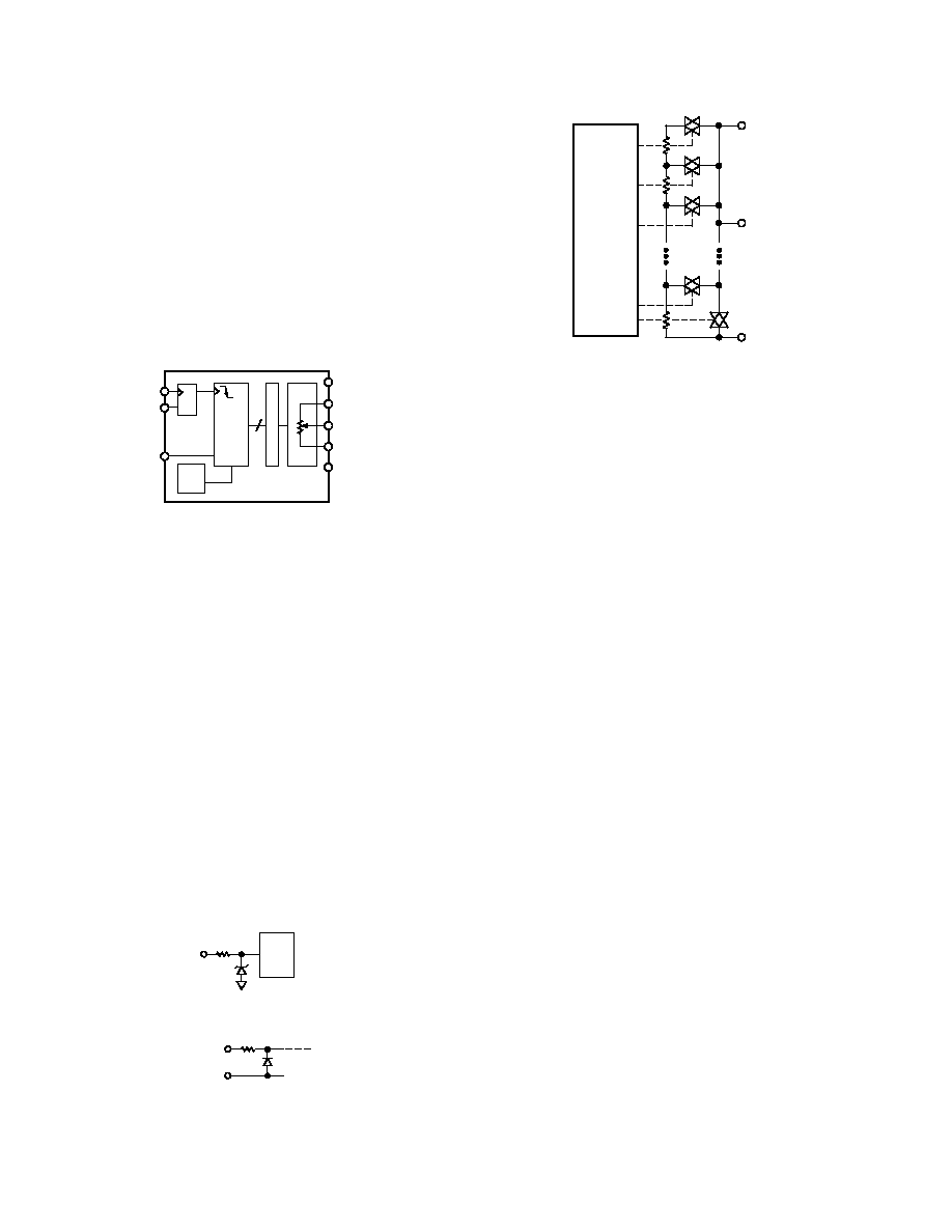
Figure 35. Block Diagram
DIGITAL INTERFACING OPERATION
The AD5220 contains a three-wire serial input interface. The
three inputs are clock (CLK), CS and UP/DOWN (U/D). The
negative-edge sensitive CLK input requires clean transitions to
avoid clocking multiple pulses into the internal UP/DOWN
counter register, see Figure 35. Standard logic families work
well. If mechanical switches are used for product evaluation
they should be debounced by a flip-flop or other suitable
means. When CS is taken active low the clock begins to incre-
ment or decrement the internal UP/DOWN counter dependent
upon the state of the U/D control pin. The UP/DOWN counter
value (D) starts at 40H at system power ON. Each new CLK
pulse will increment the value of the internal counter by one
LSB until the full scale value of 3FH is reached as long as the
U/D pin is logic high. If the U/D pin is taken to logic low the
counter will count down stopping at code 00H (zero-scale).
Additional clock pulses on the CLK pin are ignored when the
wiper is at either the 00H position or the 3FH position.
All digital inputs (CS, U/D, CLK) are protected with a series
input resistor and parallel Zener ESD structure shown in
Figure 36.
LOGIC
1k
Figure 36. Equivalent ESD Protection Digital Pins
20
A, B, W
GND
Figure 37. Equivalent ESD Protection Analog Pins
D0
D1
D2
D3
D4
D5
D6
RDAC
UP/DOWN
CNTR
&
DECODE
Wx
Bx
RS = RNOMINAL/128
RS
Ax
Figure 38. AD5220 Equivalent RDAC Circuit
PROGRAMMING THE VARIABLE RESISTOR
Rheostat Operation
The nominal resistance of the RDAC between terminals A and
B is available with values of 10 k
, 50 k, and 100 k. The
final three characters of the part number determine the nominal
resistance value, e.g., 10 k
=10; 50 k = 50; 100 k = 100.
The nominal resistance (RAB) of the VR has 128 contact points
accessed by the wiper terminal, plus the B terminal contact. At
power ON the resistance from the wiper to either end Terminal
A or B is approximately equal. Clocking the CLK pin will in-
crease the resistance from the Wiper W to Terminal B by one
unit of RS resistance (see Figure 38). The resistance RWB is
determined by the number of pulses applied to the clock pin.
Each segment of the internal resistor string has a nominal resis-
tance value of RS = RAB/128, which becomes 78 in the case of
the 10 k
AD5220BN10 product. Care should be taken to limit
the current flow between W and B in the direct contact state to
a maximum value of 5 mA to avoid degradation or possible de-
struction of the internal switch contact.
Like the mechanical potentiometer the RDAC replaces, it is
totally symmetrical (see Figure 38). The resistance between the
Wiper W and Terminal A also produces a digitally controlled
resistance RWA. When these terminals are used the B–terminal
should be tied to the wiper.
The typical part-to-part distribution of RBA is process lot depen-
dent having a
±30% variation. The change in R
BA with tempera-
ture has a 800 ppm/
°C temperature coefficient.
The RBA temperature coefficient increases as the wiper is pro-
grammed near the B-terminal due to the larger percentage con-
tribution of the wiper contact switch resistance, which has a
0.5%/
°C temperature coefficient. Figure 14 shows the effect of
the wiper contact resistance as a function of code setting. An-
other performance factor influenced by the switch contact resis-
tance is the relative linearity error performance between the
10 k
, and the 50 k or 100 k versions. The same switch
contact resistance is used in all three versions. Thus the perfor-
mance of the 50 k
and 100 k devices which have the least
impact on wiper switch resistance exhibits the best linearity
error, see Figures 7 and 8.
A
相关PDF资料 |
PDF描述 |
|---|---|
| VE-B4W-MY-F1 | CONVERTER MOD DC/DC 5.5V 50W |
| SY89297UMH | IC DELAY LINE 1024TAP 24-MLF |
| SY89296UTG | IC DELAY LINE 1024TAP 32-TQFP |
| AD5274BRMZ-100-RL7 | IC RHEOSTAT 5V 50-TP 256 10MSOP |
| VE-B4V-MY-F4 | CONVERTER MOD DC/DC 5.8V 50W |
相关代理商/技术参数 |
参数描述 |
|---|---|
| AD5220BR50 | 制造商:Analog Devices 功能描述:Digital Potentiometer 128POS 50KOhm Single 8-Pin SOIC N 制造商:Rochester Electronics LLC 功能描述:7-BIT RDAC WITH UP/DWN CONTROL - Bulk 制造商:Analog Devices 功能描述:IC DIGITAL POT. 7-BIT UP/DOWN |
| AD5220BR50-REEL7 | 制造商:Analog Devices 功能描述:Digital Potentiometer 128POS 50KOhm Single 8-Pin SOIC N T/R 制造商:Rochester Electronics LLC 功能描述:7-BIT RDAC WITH UP/DWN CONTROL - Tape and Reel |
| AD5220BRM10 | 制造商:Analog Devices 功能描述:Digital Potentiometer 128POS 10KOhm Single 8-Pin MSOP 制造商:Rochester Electronics LLC 功能描述:7-BIT RDAC WITH UP/DWN CONTROL - Bulk |
| AD5220BRM100 | 功能描述:IC DGTL POT SNGL 128POS 8USOIC RoHS:否 类别:集成电路 (IC) >> 数据采集 - 数字电位器 系列:- 标准包装:3,000 系列:DPP 接片:32 电阻(欧姆):10k 电路数:1 温度系数:标准值 300 ppm/°C 存储器类型:非易失 接口:3 线串行(芯片选择,递增,增/减) 电源电压:2.5 V ~ 6 V 工作温度:-40°C ~ 85°C 安装类型:表面贴装 封装/外壳:8-WFDFN 裸露焊盘 供应商设备封装:8-TDFN(2x3) 包装:带卷 (TR) |
| AD5220BRM100-REEL | 制造商:Rochester Electronics LLC 功能描述:- Tape and Reel 制造商:Analog Devices 功能描述: |
发布紧急采购,3分钟左右您将得到回复。