- 您现在的位置:买卖IC网 > PDF目录9425 > AD5231BRUZ10-REEL7 (Analog Devices Inc)IC DGTL POT 1024POS 10K 16TSSOP PDF资料下载
参数资料
| 型号: | AD5231BRUZ10-REEL7 |
| 厂商: | Analog Devices Inc |
| 文件页数: | 7/28页 |
| 文件大小: | 0K |
| 描述: | IC DGTL POT 1024POS 10K 16TSSOP |
| 标准包装: | 1 |
| 接片: | 1024 |
| 电阻(欧姆): | 10k |
| 电路数: | 1 |
| 温度系数: | 标准值 600 ppm/°C |
| 存储器类型: | 非易失 |
| 接口: | 4 线 SPI(芯片选择) |
| 电源电压: | 2.7 V ~ 5.5 V,±2.25 V ~ 2.75 V |
| 工作温度: | -40°C ~ 85°C |
| 安装类型: | 表面贴装 |
| 封装/外壳: | 16-TSSOP(0.173",4.40mm 宽) |
| 供应商设备封装: | 16-TSSOP |
| 包装: | 标准包装 |
| 其它名称: | AD5231BRUZ10-REEL7DKR |
第1页第2页第3页第4页第5页第6页当前第7页第8页第9页第10页第11页第12页第13页第14页第15页第16页第17页第18页第19页第20页第21页第22页第23页第24页第25页第26页第27页第28页
Data Sheet
AD5231
Rev. D | Page 15 of 28
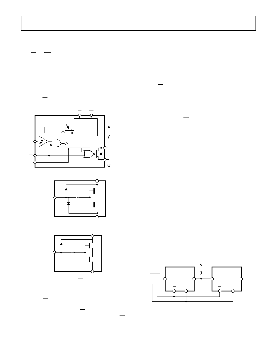
DIGITAL INPUT/OUTPUT CONFIGURATION
All digital inputs are ESD-protected, high input impedance that
can be driven directly from most digital sources. Active at logic
low, PR and WP must be tied to VDD if they are not used. No
internal pull-up resistors are present on any digital input pins.
The SDO and RDY pins are open-drain digital outputs that
need pull-up resistors only if these functions are used. A resistor
value in the range of 1 k to 10 k is a proper choice that
balances the dissipation and switching speed.
The equivalent serial data input and output logic is shown in
Figure 36. The open-drain output SDO is disabled whenever
chip-select CS is in logic high. ESD protection of the digital
inputs is shown in Figure 37 and Figure 38.
COUNTER
SERIAL
REGISTER
CLK
SDI
5V
RPULL-UP
SDO
GND
PR
WP
AD5231
CS
COMMAND
PROCESSOR
AND ADDRESS
DECODE
VALID
COMMAND
02739-
035
Figure 36. Equivalent Digital Input-Output Logic
LOGIC
PINS
VDD
GND
INPUT
300
02739-
036
Figure 37. Equivalent ESD Digital Input Protection
GND
WP
VDD
INPUT
300
02739-
037
Figure 38. Equivalent WP Input Protection
SERIAL DATA INTERFACE
The AD5231 contains a 4-wire SPI-compatible digital interface
(SDI, SDO, CS, and CLK). It uses a 24-bit serial data-word
loaded MSB first. The format of the SPI-compatible word is
shown in Table 6. The chip-select CS pin must be held low until
the complete data-word is loaded into the SDI pin. When CS
returns high, the serial data-word is decoded according to the
instructions in Table 7. The command bits (Cx) control the
operation of the digital potentiometer. The address bits (Ax)
determine which register is activated. The data bits (Dx) are the
values that are loaded into the decoded register.
The AD5231 has an internal counter that counts a multiple of
24 bits (a frame) for proper operation. For example, AD5231
works with a 48-bit word, but it cannot work properly with a
23-bit or 25-bit word. In addition, AD5231 has a subtle feature
that, if CS is pulsed without CLK and SDI, the part repeats the
previous command (except during power-up). As a result, care
must be taken to ensure that no excessive noise exists in the
CLK or CS line that might alter the effective number of bits
(ENOB) pattern. Also, to prevent data from mislocking (due
to noise, for example), the counter resets if the count is not a
multiple of four when CS goes high.
The SPI interface can be used in two slave modes: CPHA = 1,
CPOL = 1 and CPHA = 0, CPOL = 0. CPHA and CPOL refer to
the control bits that dictate SPI timing in the following
MicroConverters and microprocessors: ADuC812/ADuC824,
M68HC11, and MC68HC16R1/916R1.
DAISY-CHAIN OPERATION
The serial data output pin (SDO) serves two purposes. It can be
used to read the contents of the wiper setting and EEMEM
values using Instruction 10 and Instruction 9, respectively. The
remaining instructions (0 to 8, 11 to 15) are valid for daisy-
chaining multiple devices in simultaneous operations. Daisy-
chaining minimizes the number of port pins required from
the controlling IC (see Figure 39). The SDO pin contains an
open-drain N-Ch FET that requires a pull-up resistor if this
function is used. As shown in Figure 39, users need to tie the
SDO pin of one package to the SDI pin of the next package.
Users might need to increase the clock period, because the
pull-up resistor and the capacitive loading at the SDO to SDI
interface might require additional time delay between sub-
sequent packages. When two AD5231s are daisy-chained,
48 bits of data are required. The first 24 bits go to U2 and the
second 24 bits go to U1. The CS should be kept low until all
48 bits are clocked into their respective serial registers. The CS
is then pulled high to complete the operation.
SDI
SDO
CLK
RP
2k
C
SDI
SDO
CLK
U1
U2
AD5231
CS
+V
02739-
038
Figure 39. Daisy-Chain Configuration Using SDO
相关PDF资料 |
PDF描述 |
|---|---|
| VI-B6X-IU-F1 | CONVERTER MOD DC/DC 5.2V 200W |
| VE-23Z-MW-F4 | CONVERTER MOD DC/DC 2V 40W |
| VE-23Z-MW-F2 | CONVERTER MOD DC/DC 2V 40W |
| VI-B6W-IU-F3 | CONVERTER MOD DC/DC 5.5V 200W |
| VI-B6V-IU-F4 | CONVERTER MOD DC/DC 5.8V 200W |
相关代理商/技术参数 |
参数描述 |
|---|---|
| AD5231BRUZ50 | 功能描述:IC POT DGTL 1024POS 16-TSSOP RoHS:是 类别:集成电路 (IC) >> 数据采集 - 数字电位器 系列:- 产品培训模块:Lead (SnPb) Finish for COTS Obsolescence Mitigation Program 标准包装:1 系列:- 接片:256 电阻(欧姆):100k 电路数:1 温度系数:标准值 35 ppm/°C 存储器类型:非易失 接口:3 线串口 电源电压:2.7 V ~ 5.25 V 工作温度:-40°C ~ 85°C 安装类型:表面贴装 封装/外壳:8-WDFN 裸露焊盘 供应商设备封装:8-TDFN-EP(3x3) 包装:剪切带 (CT) 产品目录页面:1399 (CN2011-ZH PDF) 其它名称:MAX5423ETA+TCT |
| AD5231BRUZ50-REEL7 | 功能描述:IC POT DGTL 1024POS 16TSSOP RoHS:是 类别:集成电路 (IC) >> 数据采集 - 数字电位器 系列:- 标准包装:3,000 系列:DPP 接片:32 电阻(欧姆):10k 电路数:1 温度系数:标准值 300 ppm/°C 存储器类型:非易失 接口:3 线串行(芯片选择,递增,增/减) 电源电压:2.5 V ~ 6 V 工作温度:-40°C ~ 85°C 安装类型:表面贴装 封装/外壳:8-WFDFN 裸露焊盘 供应商设备封装:8-TDFN(2x3) 包装:带卷 (TR) |
| AD5232 | 制造商:AD 制造商全称:Analog Devices 功能描述:Nonvolatile Memory Digital Potentiometers |
| AD5232BRU10 | 功能描述:IC DGTL POT 256POS 10K 16TSSOP RoHS:是 类别:集成电路 (IC) >> 数据采集 - 数字电位器 系列:- 标准包装:3,300 系列:WiperLock™ 接片:257 电阻(欧姆):100k 电路数:1 温度系数:标准值 150 ppm/°C 存储器类型:易失 接口:3 线 SPI(芯片选择) 电源电压:1.8 V ~ 5.5 V 工作温度:-40°C ~ 125°C 安装类型:表面贴装 封装/外壳:8-VDFN 裸露焊盘 供应商设备封装:8-DFN-EP(3x3) 包装:带卷 (TR) |
| AD5232BRU100 | 功能描述:IC DGTL POT DUAL 256POS 16-TSSOP RoHS:否 类别:集成电路 (IC) >> 数据采集 - 数字电位器 系列:- 标准包装:2,500 系列:XDCP™ 接片:256 电阻(欧姆):100k 电路数:1 温度系数:标准值 ±300 ppm/°C 存储器类型:非易失 接口:I²C(设备位址) 电源电压:2.7 V ~ 5.5 V 工作温度:0°C ~ 70°C 安装类型:表面贴装 封装/外壳:14-TSSOP(0.173",4.40mm 宽) 供应商设备封装:14-TSSOP 包装:带卷 (TR) |
发布紧急采购,3分钟左右您将得到回复。