参数资料
| 型号: | AD5232BRU10 |
| 厂商: | Analog Devices Inc |
| 文件页数: | 10/24页 |
| 文件大小: | 0K |
| 描述: | IC DGTL POT 256POS 10K 16TSSOP |
| 标准包装: | 96 |
| 接片: | 256 |
| 电阻(欧姆): | 10k |
| 电路数: | 2 |
| 温度系数: | 标准值 600 ppm/°C |
| 存储器类型: | 非易失 |
| 接口: | 4 线 SPI(芯片选择) |
| 电源电压: | 2.7 V ~ 5.5 V,±2.25 V ~ 2.75 V |
| 工作温度: | -40°C ~ 85°C |
| 安装类型: | 表面贴装 |
| 封装/外壳: | 16-TSSOP(0.173",4.40mm 宽) |
| 供应商设备封装: | 16-TSSOP |
| 包装: | 管件 |
| 配用: | EVAL-AD5232-10EBZ-ND - BOARD EVALUATION FOR AD5232-10 |
AD5232
Data Sheet
Rev. C | Page 18 of 24
USING ADDITIONAL INTERNAL, NONVOLATILE
EEMEM
The AD5232 contains additional internal user storage registers
(EEMEM) for saving constants and other 8-bit data. Table 9
provides an address map of the internal nonvolatile storage
registers, which are shown in the functional block diagram as
EEMEM1, EEMEM2, and bytes of USER EEMEM.
Note the following about EEMEM function:
RDAC data stored in EEMEM locations are transferred to
their corresponding RDACx register at power-on or when
Command Instruction 1 and Command Instruction 8 are
executed.
USERx refers to internal nonvolatile EEMEM registers that are
available to store and retrieve constants by using Command
Instruction 3 and Command Instruction 9, respectively.
The EEMEM locations are one byte each (eight bits).
Execution of Command Instruction 1 leaves the device in
the read mode power consumption state. When the final
Command Instruction 1 is executed, the user should perform
an NOP (Command Instruction 0) to return the device to
the low power idle state.
Table 9. EEMEM Address Map
EEMEM Address
(ADDR)
EEMEM Contents of Each Device
EEMEM (ADDR)
0000
RDAC1
0001
RDAC2
0010
USER 1
0011
USER 2
0100
USER 3
0101
USER 4
***
1111
USER 14
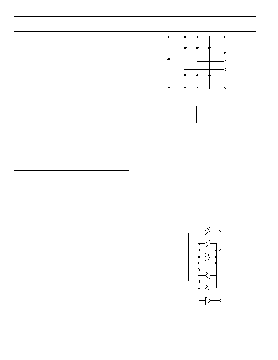
TERMINAL VOLTAGE OPERATING RANGE
The positive VDD and negative VSS power supply of the digital
potentiometer defines the boundary conditions for proper
3-terminal programmable resistance operations. Signals present
on Terminal A, Terminal B, and Wiper Terminal W that exceed
The ground pin of the AD5232 device is used primarily as
a digital ground reference that needs to be tied to the common
ground of the PCB. The digital input logic signals to the AD5232
must be referenced to the ground (GND) pin of the device and
satisfy the minimum input logic high level and the maximum
input logic low level that are defined in the Specifications section.
An internal level shift circuit between the digital interface and
the wiper switch control ensures that the common-mode voltage
range of the three terminals, Terminal A, Terminal B, and
Wiper Terminal W, extends from VSS to VDD.
VSS
VDD
A
W
B
02618-
039
Figure 39. Maximum Terminal Voltages Set by VDD and VSS
Table 10. RDAC and Digital Register Address Map
Register Address (ADDR)
Name of Register1
0000
RDAC1
0001
RDAC2
1 The RDACx registers contain data that determines the position of the
variable resistor wiper.
DETAILED POTENTIOMETER OPERATION
The actual structure of the RDACx is designed to emulate the
performance of a mechanical potentiometer. The RDACx contains
multiple strings of connected resistor segments, with an array of
analog switches that act as the wiper connection to several points
along the resistor array. The number of points is equal to the
resolution of the device. For example, the AD5232 has 256 con-
nection points, allowing it to provide better than 0.5% setability
resolution. Figure 40 provides an equivalent diagram of the con-
nections between the three terminals that make up one channel of
the RDACx. The SWA and SWB switches are always on, whereas
only one of the SW(0) to SW(2N–1) switches is on at a time,
depending on the resistance step decoded from the data bits. The
resistance contributed by RW must be accounted for in the output
resistance.
B
RS
A
W
RS = RAB/2N
RS
02618-
040
RDAC
WIPER
REGISTER
AND
DECODER
NOTES
1. DIGITAL CIRCUITRY
OMITTED FOR CLARITY
SWA
SWB
SW(2N–1)
SW(2N–2)
SW(1)
SW(2)
Figure 40. Equivalent RDAC Structure
相关PDF资料 |
PDF描述 |
|---|---|
| VI-2NW-MX-B1 | CONVERTER MOD DC/DC 5.5V 75W |
| VE-B3J-MY-F3 | CONVERTER MOD DC/DC 36V 50W |
| AD8403ARZ50 | IC DCP QUAD 50K 24-SOIC |
| VE-B3J-MY-F2 | CONVERTER MOD DC/DC 36V 50W |
| AD8403ARZ100 | IC POT DGTL 8BIT 100K 4CH 24SOIC |
相关代理商/技术参数 |
参数描述 |
|---|---|
| AD5232BRU100 | 功能描述:IC DGTL POT DUAL 256POS 16-TSSOP RoHS:否 类别:集成电路 (IC) >> 数据采集 - 数字电位器 系列:- 标准包装:2,500 系列:XDCP™ 接片:256 电阻(欧姆):100k 电路数:1 温度系数:标准值 ±300 ppm/°C 存储器类型:非易失 接口:I²C(设备位址) 电源电压:2.7 V ~ 5.5 V 工作温度:0°C ~ 70°C 安装类型:表面贴装 封装/外壳:14-TSSOP(0.173",4.40mm 宽) 供应商设备封装:14-TSSOP 包装:带卷 (TR) |
| AD5232BRU100-REEL7 | 功能描述:IC DGTL POT DUAL 256POS 16-TSSOP RoHS:否 类别:集成电路 (IC) >> 数据采集 - 数字电位器 系列:- 标准包装:3,000 系列:DPP 接片:32 电阻(欧姆):10k 电路数:1 温度系数:标准值 300 ppm/°C 存储器类型:非易失 接口:3 线串行(芯片选择,递增,增/减) 电源电压:2.5 V ~ 6 V 工作温度:-40°C ~ 85°C 安装类型:表面贴装 封装/外壳:8-WFDFN 裸露焊盘 供应商设备封装:8-TDFN(2x3) 包装:带卷 (TR) |
| AD5232BRU10-REEL7 | 功能描述:IC DGTL POT DUAL 256POS 16-TSSOP RoHS:否 类别:集成电路 (IC) >> 数据采集 - 数字电位器 系列:- 标准包装:3,000 系列:DPP 接片:32 电阻(欧姆):10k 电路数:1 温度系数:标准值 300 ppm/°C 存储器类型:非易失 接口:3 线串行(芯片选择,递增,增/减) 电源电压:2.5 V ~ 6 V 工作温度:-40°C ~ 85°C 安装类型:表面贴装 封装/外壳:8-WFDFN 裸露焊盘 供应商设备封装:8-TDFN(2x3) 包装:带卷 (TR) |
| AD5232BRU50 | 功能描述:IC DGTL POT DUAL 256POS 16-TSSOP RoHS:否 类别:集成电路 (IC) >> 数据采集 - 数字电位器 系列:- 标准包装:3,000 系列:DPP 接片:32 电阻(欧姆):10k 电路数:1 温度系数:标准值 300 ppm/°C 存储器类型:非易失 接口:3 线串行(芯片选择,递增,增/减) 电源电压:2.5 V ~ 6 V 工作温度:-40°C ~ 85°C 安装类型:表面贴装 封装/外壳:8-WFDFN 裸露焊盘 供应商设备封装:8-TDFN(2x3) 包装:带卷 (TR) |
| AD5232BRU50-REEL7 | 功能描述:IC DGTL POT DUAL 256POS 16-TSSOP RoHS:否 类别:集成电路 (IC) >> 数据采集 - 数字电位器 系列:- 标准包装:2,500 系列:XDCP™ 接片:256 电阻(欧姆):100k 电路数:1 温度系数:标准值 ±300 ppm/°C 存储器类型:非易失 接口:I²C(设备位址) 电源电压:2.7 V ~ 5.5 V 工作温度:0°C ~ 70°C 安装类型:表面贴装 封装/外壳:14-TSSOP(0.173",4.40mm 宽) 供应商设备封装:14-TSSOP 包装:带卷 (TR) |
发布紧急采购,3分钟左右您将得到回复。