- 您现在的位置:买卖IC网 > PDF目录1889 > AD5232BRU50-REEL7 (Analog Devices Inc)IC DGTL POT DUAL 256POS 16-TSSOP PDF资料下载
参数资料
| 型号: | AD5232BRU50-REEL7 |
| 厂商: | Analog Devices Inc |
| 文件页数: | 14/24页 |
| 文件大小: | 0K |
| 描述: | IC DGTL POT DUAL 256POS 16-TSSOP |
| 产品变化通告: | Product Discontinuance 27/Oct/2011 |
| 标准包装: | 1,000 |
| 接片: | 256 |
| 电阻(欧姆): | 50k |
| 电路数: | 2 |
| 温度系数: | 标准值 600 ppm/°C |
| 存储器类型: | 非易失 |
| 接口: | 4 线 SPI(芯片选择) |
| 电源电压: | 2.7 V ~ 5.5 V,±2.25 V ~ 2.75 V |
| 工作温度: | -40°C ~ 85°C |
| 安装类型: | 表面贴装 |
| 封装/外壳: | 16-TSSOP(0.173",4.40mm 宽) |
| 供应商设备封装: | 16-TSSOP |
| 包装: | 带卷 (TR) |
| 配用: | EVAL-AD5232-10EBZ-ND - BOARD EVALUATION FOR AD5232-10 |
Data Sheet
AD5232
Rev. C | Page 21 of 24
Table 16 illustrates using the left shift-by-one to change circuit
gain in 6 dB steps.
Table 16.
SDI
SDO
Action
0xC1XX
0xXXXX
Moves Wiper W2 to double the present
data value contained in the RDAC2 register
in the direction of Terminal A.
0xC1XX
0xXXXX
Moves Wiper W2 to double the present
data value contained in the RDAC2 register
in the direction of Terminal A.
Table 17 illustrates storing additional data in nonvolatile memory.
Table 17.
SDI
SDO
Action
0x3280
0xXXXX
Stores 0x80 data in spare EEMEM location,
USER1.
0x3340
0xXXXX
Stores 0x40 data in spare EEMEM location,
USER2.
Table 18 illustrates reading back data from various memory
locations.
Table 18.
SDI
SDO
Action
0x94XX
0xXXXX
Prepares data read from USER3 location.
(USER3 is already loaded with 0x80.)
0x00XX
0xXX80
Instruction 0 (NOP) sends 16-bit word out
of SDO where the last eight bits contain
the contents of USER3 location. The NOP
command ensures that the device returns
to the idle power dissipation state.
EQUIPMENT CUSTOMER START-UP SEQUENCE
FOR A PCB CALIBRATED UNIT WITH PROTECTED
SETTINGS
1.
For the PCB setting, tie WP to GND to prevent changes in
the PCB wiper set position.
2.
Set power VDD and VSS with respect to GND.
3.
As an optional step, strobe the PR pin to ensure full power-
on preset of the wiper register with EEMEM contents in
unpredictable supply sequencing environments.
FLASH/EEMEM RELIABILITY
The Flash/EE memory array on the AD5232 is fully qualified
for two key Flash/EE memory characteristics: namely, Flash/EE
memory cycling endurance and Flash/EE memory data retention.
Endurance quantifies the ability of the Flash/EE memory to be
cycled through many program, read, and erase cycles. In real
terms, a single endurance cycle is composed of four independent,
sequential events. These events are defined as follows:
1.
Initial page erase sequence
2.
Read/verify sequence
3.
Byte program sequence
4.
Second read/verify sequence
During reliability qualification, Flash/EE memory is cycled
from 0x00 to 0xFF until a first fail is recorded, signifying the
endurance limit of the on-chip Flash/EE memory.
As indicated in the Specifications section, the AD5232 Flash/EE
memory endurance qualification has been carried out in accor-
dance with JEDEC Std. 22, Method A117 over the industrial
temperature range of 40°C to +85°C. The results allow the
specification of a minimum endurance figure over supply and
temperature of 100,000 cycles, with an endurance figure of
700,000 cycles being typical of operation at 25°C.
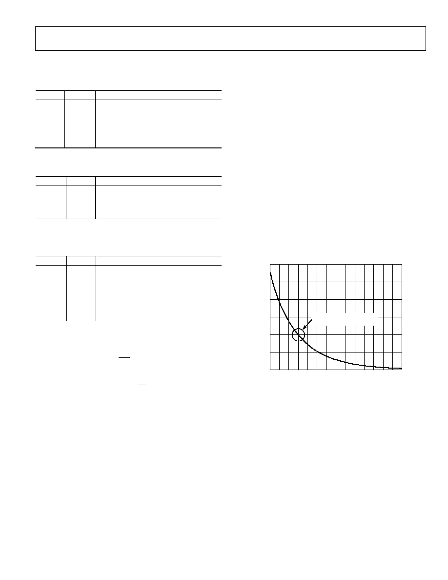
Retention quantifies the ability of the Flash/EE memory to retain
its programmed data over time. Again, the AD5232 has been
qualified in accordance with the formal JEDEC Retention
Lifetime Specification (A117) at a specific junction temperature of
TJ = 55°C. As part of this qualification procedure, the Flash/EE
memory is cycled to its specified endurance limit, as described
previously, before data retention is characterized. This means
that the Flash/EE memory is guaranteed to retain its data for
its full specified retention lifetime every time the Flash/EE
memory is repro-grammed. It should also be noted that
retention lifetime, based on an activation energy of 0.6 eV,
300
250
200
150
100
50
0
40
50
60
70
80
90
100
110
TJ JUNCTION TEMPERATURE (°C)
RE
T
E
N
T
IO
N
(
Y
ear
s)
02
61
8-
0
44
ADI TYPICAL PERFORMANCE
AT TJ = 55°C
Figure 44. Flash/EE Memory Data Retention
EVALUATION BOARD
Analog Devices, Inc., offers a user-friendly EVAL-AD5232-SDZ
evaluation kit that can be controlled by a personal computer
through a printer port. The driving program is self-contained;
no programming languages or skills are needed.
相关PDF资料 |
PDF描述 |
|---|---|
| AD5233BRUZ10 | IC DGTL POT 64POS 10K QD 24TSSOP |
| AD5235BRU25-RL7 | IC DGTL POT DUAL 1024POS 16TSSOP |
| AD5242BRU1M-REEL7 | IC DGTL POT 256POS 16-TSSOP T/R |
| AD5243BRM50-RL7 | IC DGTL POT DUAL 50K I2C 10-MSOP |
| AD5245BRJ50-R2 | IC POT DGTL 50K 256POS SOT23-8 |
相关代理商/技术参数 |
参数描述 |
|---|---|
| AD5232BRUZ10 | 功能描述:IC DGTL POT DUAL 256POS 16-TSSOP RoHS:是 类别:集成电路 (IC) >> 数据采集 - 数字电位器 系列:- 产品培训模块:Lead (SnPb) Finish for COTS Obsolescence Mitigation Program 标准包装:1 系列:- 接片:256 电阻(欧姆):100k 电路数:1 温度系数:标准值 35 ppm/°C 存储器类型:非易失 接口:3 线串口 电源电压:2.7 V ~ 5.25 V 工作温度:-40°C ~ 85°C 安装类型:表面贴装 封装/外壳:8-WDFN 裸露焊盘 供应商设备封装:8-TDFN-EP(3x3) 包装:剪切带 (CT) 产品目录页面:1399 (CN2011-ZH PDF) 其它名称:MAX5423ETA+TCT |
| AD5232BRUZ100 | 功能描述:IC DGTL POT DUAL 256POS 16-TSSOP RoHS:是 类别:集成电路 (IC) >> 数据采集 - 数字电位器 系列:- 标准包装:3,300 系列:WiperLock™ 接片:257 电阻(欧姆):100k 电路数:1 温度系数:标准值 150 ppm/°C 存储器类型:易失 接口:3 线 SPI(芯片选择) 电源电压:1.8 V ~ 5.5 V 工作温度:-40°C ~ 125°C 安装类型:表面贴装 封装/外壳:8-VDFN 裸露焊盘 供应商设备封装:8-DFN-EP(3x3) 包装:带卷 (TR) |
| AD5232BRUZ100-RL7 | 功能描述:IC DGTL POT DUAL 256POS 16-TSSOP RoHS:是 类别:集成电路 (IC) >> 数据采集 - 数字电位器 系列:- 标准包装:3,000 系列:DPP 接片:32 电阻(欧姆):10k 电路数:1 温度系数:标准值 300 ppm/°C 存储器类型:非易失 接口:3 线串行(芯片选择,递增,增/减) 电源电压:2.5 V ~ 6 V 工作温度:-40°C ~ 85°C 安装类型:表面贴装 封装/外壳:8-WFDFN 裸露焊盘 供应商设备封装:8-TDFN(2x3) 包装:带卷 (TR) |
| AD5232BRUZ10-REEL7 | 功能描述:IC POT DGTL DUAL 256POS 16TSSOP RoHS:是 类别:集成电路 (IC) >> 数据采集 - 数字电位器 系列:- 标准包装:3,000 系列:DPP 接片:32 电阻(欧姆):10k 电路数:1 温度系数:标准值 300 ppm/°C 存储器类型:非易失 接口:3 线串行(芯片选择,递增,增/减) 电源电压:2.5 V ~ 6 V 工作温度:-40°C ~ 85°C 安装类型:表面贴装 封装/外壳:8-WFDFN 裸露焊盘 供应商设备封装:8-TDFN(2x3) 包装:带卷 (TR) |
| AD5232BRUZ50 | 功能描述:IC DGTL POT 256POS 50K 16TSSOP RoHS:是 类别:集成电路 (IC) >> 数据采集 - 数字电位器 系列:- 标准包装:3,300 系列:WiperLock™ 接片:257 电阻(欧姆):100k 电路数:1 温度系数:标准值 150 ppm/°C 存储器类型:易失 接口:3 线 SPI(芯片选择) 电源电压:1.8 V ~ 5.5 V 工作温度:-40°C ~ 125°C 安装类型:表面贴装 封装/外壳:8-VDFN 裸露焊盘 供应商设备封装:8-DFN-EP(3x3) 包装:带卷 (TR) |
发布紧急采购,3分钟左右您将得到回复。