- 您现在的位置:买卖IC网 > PDF目录9425 > AD5232BRUZ10 (Analog Devices Inc)IC DGTL POT DUAL 256POS 16-TSSOP PDF资料下载
参数资料
| 型号: | AD5232BRUZ10 |
| 厂商: | Analog Devices Inc |
| 文件页数: | 13/24页 |
| 文件大小: | 0K |
| 描述: | IC DGTL POT DUAL 256POS 16-TSSOP |
| 标准包装: | 96 |
| 接片: | 256 |
| 电阻(欧姆): | 10k |
| 电路数: | 2 |
| 温度系数: | 标准值 600 ppm/°C |
| 存储器类型: | 非易失 |
| 接口: | 4 线 SPI(芯片选择) |
| 电源电压: | 2.7 V ~ 5.5 V,±2.25 V ~ 2.75 V |
| 工作温度: | -40°C ~ 85°C |
| 安装类型: | 表面贴装 |
| 封装/外壳: | 16-TSSOP(0.173",4.40mm 宽) |
| 供应商设备封装: | 16-TSSOP |
| 包装: | 管件 |
| 产品目录页面: | 787 (CN2011-ZH PDF) |
| 配用: | EVAL-AD5232-10EBZ-ND - BOARD EVALUATION FOR AD5232-10 |
AD5232
Data Sheet
Rev. C | Page 20 of 24
PROGRAMMING THE POTENTIOMETER DIVIDER
Voltage Output Operation
The digital potentiometer easily generates an output voltage pro-
portional to the input voltage applied to a given terminal. For
example, connecting Terminal A to 5 V and Terminal B to GND
produces an output voltage at the wiper that can be any value
from 0 V to 5 V. Each LSB of voltage is equal to the voltage
applied across Terminal A to Terminal B, divided by the 2N
position resolution of the potentiometer divider. The general
equation defining the output voltage with respect to ground for
any given input voltage applied to Terminal A to Terminal B is
B
AB
WA
A
AB
WB
W
V
R
D
R
V
R
D
R
D
V
×
+
×
=
)
(
)
(
)
(
(3)
where RWB(D) can be obtained from Equation 1 and RWA(D)
can be obtained from Equation 2.
Operation of the digital potentiometer in the divider mode
results in more accurate operation over temperature. Here the
output voltage is dependent on the ratio of the internal resistors,
not the absolute value; therefore, the drift improves to 15 ppm/°C.
There is no voltage polarity restriction between Terminal A,
Terminal B, and Wiper Terminal W as long as the terminal voltage
(VTERM) stays within VSS < VTERM < VDD.
OPERATION FROM DUAL SUPPLIES
The AD5232 can be operated from dual supplies, enabling
control of ground-referenced ac signals (see Figure 42 for
a typical circuit connection).
AD5232
VSS
GND
SDI
CLK
SS
SCLK
MOSI
GND
VDD
±2V p-p
±1V p-p
VDD
+2.5V
–2.5V
CS
02618-
042
MicroConverter
Figure 42. Operation from Dual Supplies
The internal parasitic capacitances and the external capacitive
loads dominate the ac characteristics of the RDACs. When
configured as a potentiometer divider, the 3 dB bandwidth of
the AD5232BRU10 (10 k resistor) measures 500 kHz at half
scale. Figure 14 provides the large signal BODE plot character-
istics of the three resistor versions: 10 k, 50 k, and 100 k (see
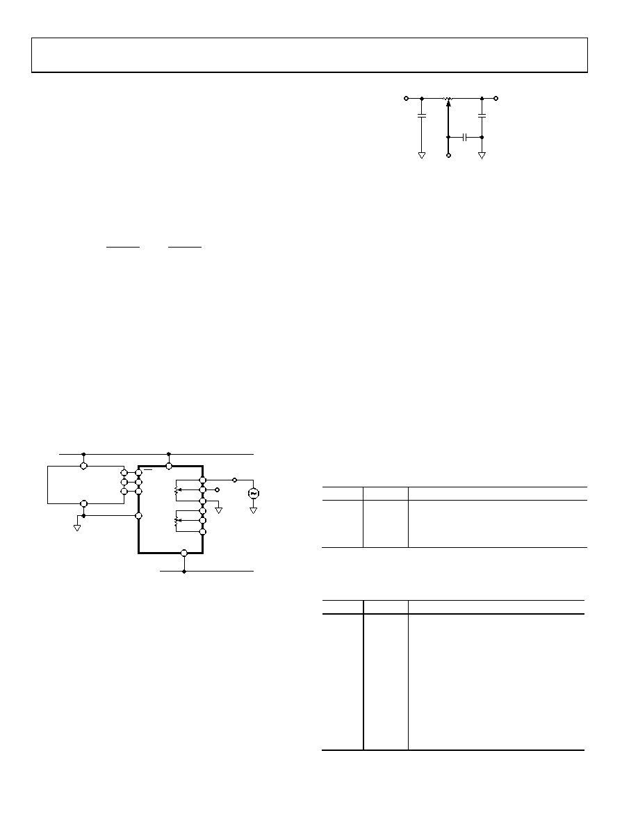
Figure 43 for a parasitic simulation model of the RDAC circuit).
A
W
02618-
043
B
RDAC
10k
CA
45pF
CB
45pF
CW
60pF
Figure 43. RDAC Circuit Simulation Model for RDACx = 10 k
The following code provides a macro model net list for the
10 k RDAC:
.PARAM DW=255, RDAC=10E3
*
.SUBCKT DPOT (A,W,B)
*
CA A 0 {45E-12}
RAW A W {(1-DW/256)*RDAC+50}
CW W 0 60E-12
RBW W B {DW/256*RDAC+50}
CB B 0 {45E-12}
*
.ENDS DPOT
APPLICATION PROGRAMMING EXAMPLES
The command sequence examples shown in Table 14 to Table 18
have been developed to illustrate a typical sequence of events
for the various features of the AD5232 nonvolatile digital poten-
tiometer. Table 14 illustrates setting two digital potentiometers
to independent data values.
Table 14.
SDI
SDO
Action
0xB140
0xXXXX
Loads 0x40 data into the RDAC2 register;
Wiper W2 moves to 1/4 full-scale position.
0xB080
0xB140
Loads 0x80 data into the RDAC1 register;
Wiper W1 moves to 1/2 full-scale position.
Table 15 illustrates the active trimming of one potentiometer,
followed by a save to nonvolatile memory (PCB calibrate).
Table 15.
SDI
SDO
Action
0xB040
0xXXXX
Loads 0x40 data into the RDAC1 register;
Wiper W1 moves to 1/4 full-scale position.
0xE0XX
0xB040
Increments the RDAC1 register by 1, to 0x41;
Wiper W1 moves one resistor segment
away from Terminal B.
0xE0XX
Increments the RDAC1 register by 1, to 0x42;
Wiper W1 moves one more resistor segment
away from Terminal B. Continue until
desired the wiper position is reached.
0x20XX
0xE0XX
Saves the RDAC1 register data into the
corresponding nonvolatile EEMEM1
memory: ADDR = 0x0.
相关PDF资料 |
PDF描述 |
|---|---|
| VI-BNM-IU-F3 | CONVERTER MOD DC/DC 10V 200W |
| VE-B24-MY-F2 | CONVERTER MOD DC/DC 48V 50W |
| VI-B23-MX-B1 | CONVERTER MOD DC/DC 24V 75W |
| AD5254BRUZ100-RL7 | IC DGTL POT 256POS 100K 20TSSOP |
| VE-B24-MY-F1 | CONVERTER MOD DC/DC 48V 50W |
相关代理商/技术参数 |
参数描述 |
|---|---|
| AD5232BRUZ100 | 功能描述:IC DGTL POT DUAL 256POS 16-TSSOP RoHS:是 类别:集成电路 (IC) >> 数据采集 - 数字电位器 系列:- 标准包装:3,300 系列:WiperLock™ 接片:257 电阻(欧姆):100k 电路数:1 温度系数:标准值 150 ppm/°C 存储器类型:易失 接口:3 线 SPI(芯片选择) 电源电压:1.8 V ~ 5.5 V 工作温度:-40°C ~ 125°C 安装类型:表面贴装 封装/外壳:8-VDFN 裸露焊盘 供应商设备封装:8-DFN-EP(3x3) 包装:带卷 (TR) |
| AD5232BRUZ100-RL7 | 功能描述:IC DGTL POT DUAL 256POS 16-TSSOP RoHS:是 类别:集成电路 (IC) >> 数据采集 - 数字电位器 系列:- 标准包装:3,000 系列:DPP 接片:32 电阻(欧姆):10k 电路数:1 温度系数:标准值 300 ppm/°C 存储器类型:非易失 接口:3 线串行(芯片选择,递增,增/减) 电源电压:2.5 V ~ 6 V 工作温度:-40°C ~ 85°C 安装类型:表面贴装 封装/外壳:8-WFDFN 裸露焊盘 供应商设备封装:8-TDFN(2x3) 包装:带卷 (TR) |
| AD5232BRUZ10-REEL7 | 功能描述:IC POT DGTL DUAL 256POS 16TSSOP RoHS:是 类别:集成电路 (IC) >> 数据采集 - 数字电位器 系列:- 标准包装:3,000 系列:DPP 接片:32 电阻(欧姆):10k 电路数:1 温度系数:标准值 300 ppm/°C 存储器类型:非易失 接口:3 线串行(芯片选择,递增,增/减) 电源电压:2.5 V ~ 6 V 工作温度:-40°C ~ 85°C 安装类型:表面贴装 封装/外壳:8-WFDFN 裸露焊盘 供应商设备封装:8-TDFN(2x3) 包装:带卷 (TR) |
| AD5232BRUZ50 | 功能描述:IC DGTL POT 256POS 50K 16TSSOP RoHS:是 类别:集成电路 (IC) >> 数据采集 - 数字电位器 系列:- 标准包装:3,300 系列:WiperLock™ 接片:257 电阻(欧姆):100k 电路数:1 温度系数:标准值 150 ppm/°C 存储器类型:易失 接口:3 线 SPI(芯片选择) 电源电压:1.8 V ~ 5.5 V 工作温度:-40°C ~ 125°C 安装类型:表面贴装 封装/外壳:8-VDFN 裸露焊盘 供应商设备封装:8-DFN-EP(3x3) 包装:带卷 (TR) |
| AD5232BRUZ50-REEL7 | 功能描述:IC POT DGTL DUAL 256POS 16TSSOP RoHS:是 类别:集成电路 (IC) >> 数据采集 - 数字电位器 系列:- 标准包装:3,000 系列:DPP 接片:32 电阻(欧姆):10k 电路数:1 温度系数:标准值 300 ppm/°C 存储器类型:非易失 接口:3 线串行(芯片选择,递增,增/减) 电源电压:2.5 V ~ 6 V 工作温度:-40°C ~ 85°C 安装类型:表面贴装 封装/外壳:8-WFDFN 裸露焊盘 供应商设备封装:8-TDFN(2x3) 包装:带卷 (TR) |
发布紧急采购,3分钟左右您将得到回复。