- 您现在的位置:买卖IC网 > PDF目录9281 > AD5235BRUZ25-RL7 (Analog Devices Inc)IC DGTL POT DUAL 1024POS 16TSSOP PDF资料下载
参数资料
| 型号: | AD5235BRUZ25-RL7 |
| 厂商: | Analog Devices Inc |
| 文件页数: | 18/32页 |
| 文件大小: | 0K |
| 描述: | IC DGTL POT DUAL 1024POS 16TSSOP |
| 产品变化通告: | Metal Edit Change 03/Feb/2012 |
| 标准包装: | 1,000 |
| 接片: | 1024 |
| 电阻(欧姆): | 25k |
| 电路数: | 2 |
| 温度系数: | 标准值 35 ppm/°C |
| 存储器类型: | 非易失 |
| 接口: | 4 线 SPI(芯片选择) |
| 电源电压: | 3 V ~ 5.5 V,±2.25 V ~ 2.75 V |
| 工作温度: | -40°C ~ 85°C |
| 安装类型: | 表面贴装 |
| 封装/外壳: | 16-TSSOP(0.173",4.40mm 宽) |
| 供应商设备封装: | 16-TSSOP |
| 包装: | 带卷 (TR) |
第1页第2页第3页第4页第5页第6页第7页第8页第9页第10页第11页第12页第13页第14页第15页第16页第17页当前第18页第19页第20页第21页第22页第23页第24页第25页第26页第27页第28页第29页第30页第31页第32页
Data Sheet
AD5235
Rev. F | Page 25 of 32
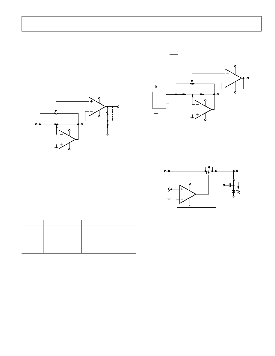
BIPOLAR PROGRAMMABLE GAIN AMPLIFIER
For applications requiring bipolar gain, Figure 51 shows one
implementation. Digital Potentiometer U1 sets the adjustment
range; the wiper voltage (VW2) can, therefore, be programmed
(A2) as a noninverting amplifier that yields a transfer function of
K
D2
R1
R2
V
I
O
)
1
(
1024
1
(4)
where K is the ratio of RWB1/RWA1 set by U1.
V+
V–
OP2177
AD5235
VO
V+
V–
OP2177
AD5235
VI
A1
W1
B1
–KVI
A2
B2
W1
VDD
VSS
R1
R2
VDD
VSS
A1
U2
A2
U1
02
81
6-
0
50
C
Figure 51. Bipolar Programmable Gain Amplifier
In the simpler (and much more usual) case where K = 1, VO is
simplified to
I
O
V
D
R1
R2
V
1
1024
2
1
(5)
Table 21 shows the result of adjusting D2, with OP2177 (A2)
configured as a unity gain, a gain of 2, and a gain of 10. The
result is a bipolar amplifier with linearly programmable gain
and 1024-step resolution.
Table 21. Result of Bipolar Gain Amplifier
D2
R1 = ∞, R2 = 0
R1 = R2
R2 = 9 × R1
0
1
2
10
256
0.5
1
5
512
0
768
0.5
1
5
1023
0.992
1.984
9.92
10-BIT BIPOLAR DAC
If the circuit in Figure 51 is changed with the input taken from a
precision reference, U1 is set to midscale, and AD8552 (A2) is
configured as a buffer, a 10-bit bipolar DAC can be realized (as
shown in Figure 52). Compared to the conventional DAC, this
circuit offers comparable resolution but not the precision because
of the wiper resistance effects. Degradation of the nonlinearity
and temperature coefficient is prominent near the low values
of the adjustment range. Alternatively, this circuit offers a unique
nonvolatile memory feature that, in some cases, outweighs any
shortfalls in precision.
Without consideration of the wiper resistance, the output of this
circuit is approximately
REF
O
V
D
V
1
1024
2
(6)
V+
V–
AD8552
VO
V+
V–
AD8552
–2.5VREF
B2
U1 = U2 = AD5235
A2
A1
B1
W2
A1
W1
U1
U2
+2.5VREF
VIN VOUT
TRIM
5
GND
2
6
U3
ADR421
+2.5V
–2.5V
+2.5V
A2
VI
02
81
6-
05
1
U1 = MIDSCALE
Figure 52. 10-Bit Bipolar DAC
PROGRAMMABLE VOLTAGE SOURCE WITH
BOOSTED OUTPUT
For applications that require high current adjustment, such as a
laser diode driver or tunable laser, a boosted voltage source can
be considered (see Figure 53).
AD5235
V+
V–
W
AD8601
VO
A
B
VI
2N7002
RBIAS
SIGNAL CC
LD
IL
02
81
6-
05
2
U2
Figure 53. Programmable Booster Voltage Source
In this circuit, the inverting input of the op amp forces VO to be
equal to the wiper voltage set by the digital potentiometer. The
load current is then delivered by the supply via the N-Ch FET N1
(VI VO) × IL power. This circuit can source a 100 mA maximum
with a 5 V supply.
For precision applications, a voltage reference, such as ADR421,
potentiometer.
相关PDF资料 |
PDF描述 |
|---|---|
| VI-2TP-MW | CONVERTER MOD DC/DC 13.8V 100W |
| DS1135Z-12+T&R | IC DELAY LINE 12NS 8-SOIC |
| DS1135Z-20+T&R | IC DELAY LINE 20NS 8-SOIC |
| DS1135Z-10+T&R | IC DELAY LINE 10NS 8-SOIC |
| DS1100LU-25+T | IC DELAY LINE 5TAP 25NS 8-USOP |
相关代理商/技术参数 |
参数描述 |
|---|---|
| AD5235-EP | 制造商:AD 制造商全称:Analog Devices 功能描述:Nonvolatile Memory, Dual 1024-Position Digital Potentiometer |
| AD5235EVAL | 制造商:Analog Devices 功能描述:DUAL 10BIT SPI EVAL BOARD - Bulk |
| AD5235EVAL25 | 制造商:Analog Devices 功能描述:Evaluation Board For 1024-Position Digital Potentiometer 制造商:Analog Devices 功能描述:DUAL 10BIT SPI EVAL BOARD - Bulk |
| AD5235EVAL250 | 制造商:Analog Devices 功能描述:DUAL 10BIT SPI EVAL BOARD - Bulk |
| AD523BS | 制造商:POP 功能描述: |
发布紧急采购,3分钟左右您将得到回复。