- 您现在的位置:买卖IC网 > PDF目录373873 > AD5242BR100 (ANALOG DEVICES INC) Audio digital potentiometers PDF资料下载
参数资料
| 型号: | AD5242BR100 |
| 厂商: | ANALOG DEVICES INC |
| 元件分类: | 数字电位计 |
| 英文描述: | Audio digital potentiometers |
| 中文描述: | DUAL 100K DIGITAL POTENTIOMETER, 2-WIRE SERIAL CONTROL INTERFACE, 256 POSITIONS, PDSO16 |
| 封装: | MS-012AC, SOIC-16 |
| 文件页数: | 11/16页 |
| 文件大小: | 394K |
| 代理商: | AD5242BR100 |
REV. B
–11–
AD5241/AD5242
Pin except that
SHDN
Pin reacts to active low. The follow-
ing two bits are O
2
and O
1
. They are extra programmable
logic outputs that users can use to drive other digital loads,
logic gates, LED drivers, analog switches, and the like. The
three LSBs are Don’t Care. See Figure 2.
3. After acknowledging the Instruction Byte, the last byte in
Write Mode is the Data Byte, Frame 3. Data is transmitted
over the serial bus in sequences of nine clock pulses (eight
data bits followed by an Acknowledge Bit). The transitions
on the SDA line must occur during the low period of SCL
and remain stable during the high period of SCL (Figure 2).
4. Unlike the Write Mode, the Data Byte follows immediately
after the acknowledgment of the Slave Address Byte in Read
Mode, Frame 2. Data is transmitted over the serial bus
in sequences of nine clock pulses (slightly different than the
Write Mode, there are eight data bits followed by a No
Acknowledge logic 1 Bit in Read Mode). Similarly, the transi-
tions on the SDA line must occur during the low period of
SCL and remain stable during the high period of SCL. See
Figure 3.
5. When all Data Bits have been read or written, a STOP condi-
tion is established by the master. A STOP condition is
defined as a low-to-high transition on the SDA line while
SCL is high. In Write Mode, the master will pull the SDA line
high during the tenth clock pulse to establish a STOP con-
dition (see Figure 2). In Read Mode, the master will issue a
No Acknowledge for the ninth clock pulse (i.e., the SDA
line remains high). The master will then bring the SDA
line low before the tenth clock pulse, which goes high to
establish a STOP condition (see Figure 3).
A repeated Write function gives the user flexibility to update the
RDAC output a number of times after addressing and instruct-
ing the part only once. During the Write cycle, each Data Byte
will update the RDAC output. For example, after the RDAC
has acknowledged its Slave Address and Instruction Bytes, the
RDAC output will be updated. If another byte is written to the
RDAC while it is still addressed to a specific slave device with
the same instruction, this byte will update the output of the
selected slave device. If different instructions are needed, the
Write Mode has to start a whole new sequence with a new Slave
Address, Instruction, and Data Bytes transferred again. Simi-
larly, a repeated Read function of the RDAC is also allowed.
READBACK RDAC VALUE
Specific to the AD5242 dual-channel device, the channel of inter-
est is the one that was previously selected in the Write Mode.
In addition, to read both RDAC values consecutively, users
have to perform two write-read cycles. For example, users may
first specify the RDAC1 subaddress in the Write Mode (it is not
necessary to issue the Data Byte and the STOP condition), then
change to the Read Mode and read the RDAC1 value. To con-
tinue reading the RDAC2 value, users have to switch back to
the Write Mode and specify the subaddress, then switch once
again to the Read Mode and read the RDAC2 value. It is not
necessary to issue the Write Mode Data Byte or the first stop
condition for this operation. Users should refer to Figures 2 and
3 for the programming format.
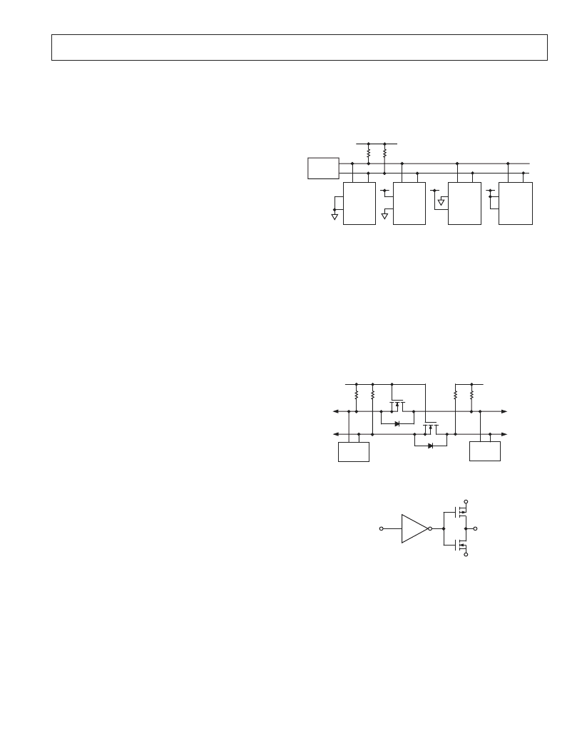
MULTIPLE DEVICES ON ONE BUS
Figure 5 shows four AD5242 devices on the same serial bus.
Each has a different slave address since the state of their AD0
and AD1 Pins are different. This allows each RDAC within
each device to be written to or read from independently. The
master device output bus line drivers are open-drain pull-
downs in a fully I
2
C compatible interface. Note, a device will be
addressed properly only if the bit information of AD0 and
AD1 in the Slave Address Byte matches with the logic inputs at
pins AD0 and AD1 of that particular device.
SDA SCL
AD5242
AD1
AD0
SDA
SCL
R
P
R
P
SDA SCL
AD5242
V
DD
AD1
AD0
SDA SCL
AD1
AD0
AD5242
V
DD
SDA SCL
AD5242
V
DD
AD1
AD0
MASTER
5V
Figure 5. Multiple AD5242 Devices on One Bus
LEVEL-SHIFT FOR BIDIRECTIONAL INTERFACE
While most old systems may be operated at one voltage, a new
component may be optimized at another. When they operate the
same signal at two different voltages, a proper method of level-
shifting is needed. For instance, one can use a 3.3 V E
2
PROM
to interface with a 5 V digital potentiometer. A level-shift scheme
is needed in order to enable a bidirectional communication so
that the setting of the digital potentiometer can be stored to and
retrieved from the E
2
PROM. Figure 6 shows one of the tech-
niques. M1 and M2 can be N-Ch FETs 2N7002 or low threshold
FDV301N if V
DD
falls below 2.5 V.
R
P
R
P
S
D
G
M1
S
D
G
M2
3.3V
E
2
PROM
R
P
R
P
5V
AD5242
SCL2
SDA2
V
DD2
= 5V
SCL1
SDA1
V
DD2
= 3.3V
Figure 6. Level-Shift for Different Voltage Devices Operation
IN
1
2
V
DD
O1
V
SS
M
P
M
N
O1 DATA IN FRAME 2
Figure 7. Output Stage of Logic Output O
1
ADDITIONAL PROGRAMMABLE LOGIC OUTPUT
AD5241/AD5242 feature additional programmable logic out-
puts, O
1
and O
2,
that can be used to drive digital load, analog
switches, and logic gates. They can also be used as self-con-
tained shutdown as preset to logic 0 feature which will be
explained later. O
1
and O
2
default to logic 0 during power-up.
The logic states of O
1
and O
2
can be programmed in Frame 2
under the Write Mode (see Figure 2). Figure 7 shows the out-
put stage of O
1
which employs large P and N channel MOSFETs
in push-pull configuration. As shown, the output will be equal to
V
DD
or V
SS
, and these logic outputs have adequate current driving
capability to drive milliamperes of load.
相关PDF资料 |
PDF描述 |
|---|---|
| AD5242BR100-REEL7 | Audio digital potentiometers |
| AD5242BRU10-REEL7 | Audio digital potentiometers |
| AD5242BRU100-REEL7 | Audio digital potentiometers |
| AD5241BR1M | Audio digital potentiometers |
| AD5241BRU1M-REEL7 | Audio digital potentiometers |
相关代理商/技术参数 |
参数描述 |
|---|---|
| AD5242BR100-REEL7 | 功能描述:IC DGTL POT 256POS 16-SOIC T/R RoHS:否 类别:集成电路 (IC) >> 数据采集 - 数字电位器 系列:- 标准包装:2,500 系列:XDCP™ 接片:256 电阻(欧姆):100k 电路数:1 温度系数:标准值 ±300 ppm/°C 存储器类型:非易失 接口:I²C(设备位址) 电源电压:2.7 V ~ 5.5 V 工作温度:0°C ~ 70°C 安装类型:表面贴装 封装/外壳:14-TSSOP(0.173",4.40mm 宽) 供应商设备封装:14-TSSOP 包装:带卷 (TR) |
| AD5242BR10-REEL7 | 功能描述:IC DGTL POT 256POS 16-SOIC T/R RoHS:否 类别:集成电路 (IC) >> 数据采集 - 数字电位器 系列:- 标准包装:3,000 系列:DPP 接片:32 电阻(欧姆):10k 电路数:1 温度系数:标准值 300 ppm/°C 存储器类型:非易失 接口:3 线串行(芯片选择,递增,增/减) 电源电压:2.5 V ~ 6 V 工作温度:-40°C ~ 85°C 安装类型:表面贴装 封装/外壳:8-WFDFN 裸露焊盘 供应商设备封装:8-TDFN(2x3) 包装:带卷 (TR) |
| AD5242BR1M | 功能描述:IC DGTL POT 256POS 16-SOIC RoHS:否 类别:集成电路 (IC) >> 数据采集 - 数字电位器 系列:- 标准包装:2,500 系列:XDCP™ 接片:256 电阻(欧姆):100k 电路数:1 温度系数:标准值 ±300 ppm/°C 存储器类型:非易失 接口:I²C(设备位址) 电源电压:2.7 V ~ 5.5 V 工作温度:0°C ~ 70°C 安装类型:表面贴装 封装/外壳:14-TSSOP(0.173",4.40mm 宽) 供应商设备封装:14-TSSOP 包装:带卷 (TR) |
| AD5242BR1M-REEL7 | 制造商:未知厂家 制造商全称:未知厂家 功能描述:DIGITAL POTENTIOMETER|SOP|16PIN|PLASTIC |
| AD5242BRU10 | 功能描述:IC DGTL POT 256POS 16-TSSOP RoHS:否 类别:集成电路 (IC) >> 数据采集 - 数字电位器 系列:- 标准包装:2,500 系列:XDCP™ 接片:256 电阻(欧姆):100k 电路数:1 温度系数:标准值 ±300 ppm/°C 存储器类型:非易失 接口:I²C(设备位址) 电源电压:2.7 V ~ 5.5 V 工作温度:0°C ~ 70°C 安装类型:表面贴装 封装/外壳:14-TSSOP(0.173",4.40mm 宽) 供应商设备封装:14-TSSOP 包装:带卷 (TR) |
发布紧急采购,3分钟左右您将得到回复。