参数资料
| 型号: | AD5246BKS5-R2 |
| 厂商: | Analog Devices Inc |
| 文件页数: | 6/16页 |
| 文件大小: | 0K |
| 描述: | IC POT DGTL 5K 128POS SC70-6 |
| 标准包装: | 1 |
| 接片: | 128 |
| 电阻(欧姆): | 5k |
| 电路数: | 1 |
| 温度系数: | 标准值 45 ppm/°C |
| 存储器类型: | 易失 |
| 接口: | I²C |
| 电源电压: | 2.7 V ~ 5.5 V |
| 工作温度: | -40°C ~ 125°C |
| 安装类型: | 表面贴装 |
| 封装/外壳: | 6-TSSOP,SC-88,SOT-363 |
| 供应商设备封装: | SC-70-6 |
| 包装: | 剪切带 (CT) |
| 其它名称: | AD5246BKS5-R2CT |
AD5246
Data Sheet
Rev. C | Page 14 of 16
A repeated write function gives the user flexibility to update the
RDAC output a number of times after addressing the part only
once. For example, after the RDAC has acknowledged its slave
address in write mode, the RDAC output updates on each succes-
sive byte. If different instructions are needed, the write/read mode
has to start again with a new slave address and data byte.
Similarly, a repeated read function of the RDAC is also allowed.
LEVEL SHIFTING FOR BIDIRECTIONAL INTERFACE
While most legacy systems may be operated at one voltage,
a new component may be optimized at another. When two
systems operate the same signal at two different voltages, proper
level shifting is needed. For instance, one can use a 1.8 V
E2PROM to interface with a 5 V digital potentiometer. A level
shifting scheme is needed to enable a bidirectional communi-
cation so that the setting of the digital potentiometer can be
one of the implementations. M1 and M2 can be any N channel
signal FETs, or if VDD falls below 2.5 V, M1 and M2 can be low
threshold FETs such as the FDV301N.
E2PROM
AD5246
SDA1
SCL1
D
G
RP
1.8V
5V
S
M1
SCL2
SDA2
RP
G
S
M2
VDD1 = 1.8V
VDD2 = 5V
D
03875-011
Figure 30. Level Shifting for Operation at Different Potentials
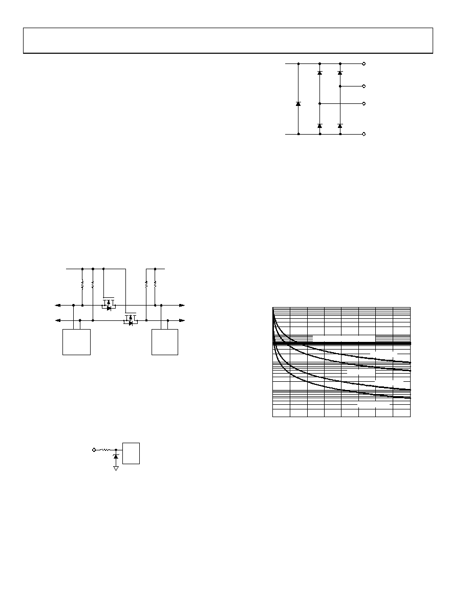
ESD PROTECTION
All digital inputs are protected with a series input resistor
and parallel Zener ESD structures, as shown in Figure 31.
This applies to the digital input pins SDA and SCL.
LOGIC
340
GND
03875-002
Figure 31. ESD Protection of Digital Pins
TERMINAL VOLTAGE OPERATING RANGE
The AD5246 VDD and GND power supply defines the boundary
conditions for proper 3-terminal digital potentiometer
operation. Supply signals present on Terminal B and
Terminal W that exceed VDD or GND are clamped by
the internal forward biased diodes (see Figure 32).
B
VDD
W
GND
03875-016
Figure 32. Maximum Terminal Voltages Set by VDD and GND
MAXIMUM OPERATING CURRENT
At low code values, the user should be aware that due to low
resistance values, the current through the RDAC may exceed
the 5 mA limit. In Figure 33, a 5 V supply is placed on the
wiper, and the current through Terminal W and Terminal B is
plotted with respect to code. A line is also drawn denoting the
5 mA current limit. Note that at low code values (particularly
for the 5 kΩ and 10 kΩ options), the current level increases
significantly. Care should be taken to limit the current flow
between W and B in this state to a maximum continuous
current of 5 mA and a maximum pulse current of no more than
20 mA. Otherwise, degradation or possible destruction of the
internal switch contacts can occur.
CODE (Decimal)
IWB
CURRENT
(mA)
0
0.01
0.1
1
10
16
32
48
64
80
96
112
128
100
5mA CURRENT LIMIT
RAB = 5k
RAB = 10k
RAB = 100k
RAB = 50k
03875-034
Figure 33. Maximum Operating Current
POWER-UP SEQUENCE
Since the ESD protection diodes limit the voltage compliance
at Terminal B and Terminal W (see Figure 32), it is important
to power VDD/GND before applying any voltage to Terminal B
and Terminal W; otherwise, the diode is forward biased such
that VDD is powered unintentionally and may affect the rest of
the user’s circuit. The ideal power-up sequence is in the follow-
ing order: GND, VDD, digital inputs, and then VB/VW. The
relative order of powering VB and VW and the digital inputs
is not important, providing they are powered after VDD/GND.
相关PDF资料 |
PDF描述 |
|---|---|
| VI-BWN-MY-F4 | CONVERTER MOD DC/DC 18.5V 50W |
| AD5246BKS10-R2 | IC POT DGTL 10K 128POS SC70-6 |
| AD5246BKS100-R2 | IC POT DGTL 100K 128POS SC70-6 |
| 7WBD383AMUTCG | IC BUS SWITCH 1X1 8UQFN |
| VI-BWN-MY-F3 | CONVERTER MOD DC/DC 18.5V 50W |
相关代理商/技术参数 |
参数描述 |
|---|---|
| AD5246BKS5-RL7 | 制造商:Analog Devices 功能描述:Digital Potentiometer 128POS 5KOhm Single 6-Pin SC-70 T/R 制造商:Rochester Electronics LLC 功能描述:7-BIT I2C DIG TRIMMER - Tape and Reel |
| AD5246BKSZ100-R2 | 功能描述:IC DGTL RES 100K I2C SC70-6 RoHS:是 类别:集成电路 (IC) >> 数据采集 - 数字电位器 系列:- 标准包装:3,000 系列:DPP 接片:32 电阻(欧姆):10k 电路数:1 温度系数:标准值 300 ppm/°C 存储器类型:非易失 接口:3 线串行(芯片选择,递增,增/减) 电源电压:2.5 V ~ 6 V 工作温度:-40°C ~ 85°C 安装类型:表面贴装 封装/外壳:8-WFDFN 裸露焊盘 供应商设备封装:8-TDFN(2x3) 包装:带卷 (TR) |
| AD5246BKSZ100-RL7 | 功能描述:IC DGTL RES 100K I2C SC70-6 RoHS:是 类别:集成电路 (IC) >> 数据采集 - 数字电位器 系列:- 产品培训模块:Lead (SnPb) Finish for COTS Obsolescence Mitigation Program 标准包装:1 系列:- 接片:256 电阻(欧姆):100k 电路数:1 温度系数:标准值 35 ppm/°C 存储器类型:非易失 接口:3 线串口 电源电压:2.7 V ~ 5.25 V 工作温度:-40°C ~ 85°C 安装类型:表面贴装 封装/外壳:8-WDFN 裸露焊盘 供应商设备封装:8-TDFN-EP(3x3) 包装:剪切带 (CT) 产品目录页面:1399 (CN2011-ZH PDF) 其它名称:MAX5423ETA+TCT |
| AD5246BKSZ10-R2 | 制造商:Analog Devices 功能描述:128 POSITION I2C COMPATIBLE PROGRAMMABLE RESISTOR IN SC70 PK - Tape and Reel |
| AD5246BKSZ10-RL7 | 功能描述:IC POT DGTL RES 128POS SC70-6 RoHS:是 类别:集成电路 (IC) >> 数据采集 - 数字电位器 系列:- 产品培训模块:Lead (SnPb) Finish for COTS Obsolescence Mitigation Program 标准包装:1 系列:- 接片:256 电阻(欧姆):100k 电路数:1 温度系数:标准值 35 ppm/°C 存储器类型:非易失 接口:3 线串口 电源电压:2.7 V ~ 5.25 V 工作温度:-40°C ~ 85°C 安装类型:表面贴装 封装/外壳:8-WDFN 裸露焊盘 供应商设备封装:8-TDFN-EP(3x3) 包装:剪切带 (CT) 产品目录页面:1399 (CN2011-ZH PDF) 其它名称:MAX5423ETA+TCT |
发布紧急采购,3分钟左右您将得到回复。