- 您现在的位置:买卖IC网 > PDF目录373873 > AD5246BKS5-RL7 (ANALOG DEVICES INC) 128-Position I2C Compatible Digital Resistor PDF资料下载
参数资料
| 型号: | AD5246BKS5-RL7 |
| 厂商: | ANALOG DEVICES INC |
| 元件分类: | 数字电位计 |
| 英文描述: | 128-Position I2C Compatible Digital Resistor |
| 中文描述: | 5K DIGITAL POTENTIOMETER, 2-WIRE SERIAL CONTROL INTERFACE, 128 POSITIONS, PDSO6 |
| 封装: | 2 X 2.10 MM, MO-203AB, SC-70, 6 PIN |
| 文件页数: | 13/20页 |
| 文件大小: | 991K |
| 代理商: | AD5246BKS5-RL7 |
AD5246
I
2
C COMPATIBLE 2-WIRE SERIAL BUS
The first byte of the AD5246 is a slave address byte (see
and
). It has a 7-bit slave address and a R/W bit. The
seven MSBs of the slave address are 0101110 followed by 0 for a
write command or 1 to place the device in read mode.
Table 5
able 5
Table 6
The 2-wire I
2
C serial bus protocol operates as follows:
1.
The master initiates data transfer by establishing a START
condition, which is when a high-to-low transition on the
SDA line occurs while SCL is high (see
following byte is the slave address byte, which consists of
the 7-bit slave address followed by an R/W bit (this bit
determines whether data will be read from or written to
the slave device).
). The
Figure 26
Figure 26
The slave whose address corresponds to the transmitted
address responds by pulling the SDA line low during the
ninth clock pulse (this is termed the acknowledge bit). At
this stage, all other devices on the bus remain idle while the
selected device waits for data to be written to or read from
its serial register. If the R/W bit is high, the master will read
from the slave device. On the other hand, if the R/W bit is
low, the master will write to the slave device.
2.
In write mode, after acknowledgement of the slave address
byte, the next byte is the data byte. Data is transmitted over
the serial bus in sequences of nine clock pulses (eight data
bits followed by an acknowledge bit). The transitions on
the SDA line must occur during the low period of SCL and
remain stable during the high period of SCL (see T
).
3.
In read mode, after acknowledgment of the slave address
byte, data is received over the serial bus in sequences of
nine clock pulses (a slight difference from the write mode
where eight data bits are followed by an acknowledge bit).
Similarly, the transitions on the SDA line must occur
during the low period of SCL and remain stable during the
high period of SCL (see
Figure 27
).
Figure 27
4.
When all data bits have been read or written, a STOP
condition is established by the master. A STOP condition is
defined as a low-to-high transition on the SDA line while
SCL is high. In write mode, the master will pull the SDA
line high during the tenth clock pulse to establish a STOP
condition (see
). In read mode, the master will
issue a No Acknowledge for the ninth clock pulse (i.e., the
SDA line remains high). The master will then bring the
SDA line low before the tenth clock pulse, which goes high
to establish a STOP condition (see
).
A repeated write function gives the user flexibility to update the
RDAC output a number of times after addressing the part only
once. For example, after the RDAC has acknowledged its slave
address in write mode, the RDAC output will update on each
successive byte. If different instructions are needed, write/read
mode has to start again with a new slave address and data byte.
Similarly, a repeated read function of the RDAC is also allowed.
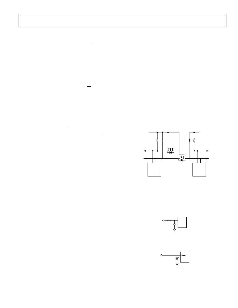
LEVEL SHIFTING FOR BIDIRECTIONAL INTERFACE
While most legacy systems may be operated at one voltage, a
new component may be optimized at another. When two
systems operate the same signal at two different voltages, proper
level shifting is needed. For instance, one can use a 3.3 V
E
2
PROM to interface with a 5 V digital potentiometer. A level
shifting scheme is needed to enable a bidirectional communi-
cation so that the setting of the digital potentiometer can be
stored to and retrieved from the E
2
PROM. F
of the implementations. M1 and M2 can be any N channel
signal FETs, or if V
DD
falls below 2.5 V, M1 and M2 can be low
threshold FETs such as the FDV301N.
shows one
igure 29
Figure 29. Level Shifting for Operation at Different Potentials
E
2
PROM
AD5246
SDA1
SCL1
D
G
R
P
R
P
3.3V
5V
S
M1
SCL2
SDA2
R
P
R
P
G
S
M2
V
DD1
= 3.3V
V
DD2=
5V
D
0
ESD PROTECTION
All digital inputs are protected with a series input resistor and
parallel Zener ESD structures shown in F
This applies to the digital input pins SDA and SCL.
and
.
igure 30
Figure 30. ESD Protection of Digital Pins
Figure 31
Figure 31. ESD Protection of Resistor Terminals
LOGIC
340
GND
0
B,W
0
GND
Rev. 0 | Page 13 of 20
相关PDF资料 |
PDF描述 |
|---|---|
| AD5246BKS50-R2 | 128-Position I2C Compatible Digital Resistor |
| AD5246BKS50-RL7 | 128-Position I2C Compatible Digital Resistor |
| AD5246EVAL | 128-Position I2C Compatible Digital Resistor |
| AD5247BKS100-RL7 | 128-Position I2C Compatible Digital Potentiometer |
| AD5247BKS5-R2 | 128-Position I2C Compatible Digital Potentiometer |
相关代理商/技术参数 |
参数描述 |
|---|---|
| AD5246BKSZ100-R2 | 功能描述:IC DGTL RES 100K I2C SC70-6 RoHS:是 类别:集成电路 (IC) >> 数据采集 - 数字电位器 系列:- 标准包装:3,000 系列:DPP 接片:32 电阻(欧姆):10k 电路数:1 温度系数:标准值 300 ppm/°C 存储器类型:非易失 接口:3 线串行(芯片选择,递增,增/减) 电源电压:2.5 V ~ 6 V 工作温度:-40°C ~ 85°C 安装类型:表面贴装 封装/外壳:8-WFDFN 裸露焊盘 供应商设备封装:8-TDFN(2x3) 包装:带卷 (TR) |
| AD5246BKSZ100-RL7 | 功能描述:IC DGTL RES 100K I2C SC70-6 RoHS:是 类别:集成电路 (IC) >> 数据采集 - 数字电位器 系列:- 产品培训模块:Lead (SnPb) Finish for COTS Obsolescence Mitigation Program 标准包装:1 系列:- 接片:256 电阻(欧姆):100k 电路数:1 温度系数:标准值 35 ppm/°C 存储器类型:非易失 接口:3 线串口 电源电压:2.7 V ~ 5.25 V 工作温度:-40°C ~ 85°C 安装类型:表面贴装 封装/外壳:8-WDFN 裸露焊盘 供应商设备封装:8-TDFN-EP(3x3) 包装:剪切带 (CT) 产品目录页面:1399 (CN2011-ZH PDF) 其它名称:MAX5423ETA+TCT |
| AD5246BKSZ10-R2 | 制造商:Analog Devices 功能描述:128 POSITION I2C COMPATIBLE PROGRAMMABLE RESISTOR IN SC70 PK - Tape and Reel |
| AD5246BKSZ10-RL7 | 功能描述:IC POT DGTL RES 128POS SC70-6 RoHS:是 类别:集成电路 (IC) >> 数据采集 - 数字电位器 系列:- 产品培训模块:Lead (SnPb) Finish for COTS Obsolescence Mitigation Program 标准包装:1 系列:- 接片:256 电阻(欧姆):100k 电路数:1 温度系数:标准值 35 ppm/°C 存储器类型:非易失 接口:3 线串口 电源电压:2.7 V ~ 5.25 V 工作温度:-40°C ~ 85°C 安装类型:表面贴装 封装/外壳:8-WDFN 裸露焊盘 供应商设备封装:8-TDFN-EP(3x3) 包装:剪切带 (CT) 产品目录页面:1399 (CN2011-ZH PDF) 其它名称:MAX5423ETA+TCT |
| AD5246BKSZ50-RL7 | 功能描述:IC POT DGTL RES 128POS SC70-6 RoHS:是 类别:集成电路 (IC) >> 数据采集 - 数字电位器 系列:- 产品培训模块:Lead (SnPb) Finish for COTS Obsolescence Mitigation Program 标准包装:1 系列:- 接片:256 电阻(欧姆):100k 电路数:1 温度系数:标准值 35 ppm/°C 存储器类型:非易失 接口:3 线串口 电源电压:2.7 V ~ 5.25 V 工作温度:-40°C ~ 85°C 安装类型:表面贴装 封装/外壳:8-WDFN 裸露焊盘 供应商设备封装:8-TDFN-EP(3x3) 包装:剪切带 (CT) 产品目录页面:1399 (CN2011-ZH PDF) 其它名称:MAX5423ETA+TCT |
发布紧急采购,3分钟左右您将得到回复。