- 您现在的位置:买卖IC网 > PDF目录373874 > AD5254BRU100-RL7 (ANALOG DEVICES INC) Dual, 256-Tap, Nonvolatile, I2C-Interface, Digital Potentiometers PDF资料下载
参数资料
| 型号: | AD5254BRU100-RL7 |
| 厂商: | ANALOG DEVICES INC |
| 元件分类: | 数字电位计 |
| 英文描述: | Dual, 256-Tap, Nonvolatile, I2C-Interface, Digital Potentiometers |
| 中文描述: | QUAD 100K DIGITAL POTENTIOMETER, 2-WIRE SERIAL CONTROL INTERFACE, 256 POSITIONS, PDSO20 |
| 封装: | MO-153AC, TSSOP-20 |
| 文件页数: | 19/28页 |
| 文件大小: | 834K |
| 代理商: | AD5254BRU100-RL7 |
第1页第2页第3页第4页第5页第6页第7页第8页第9页第10页第11页第12页第13页第14页第15页第16页第17页第18页当前第19页第20页第21页第22页第23页第24页第25页第26页第27页第28页
AD5253/AD5254
I
2
C COMPATIBLE 2-WIRE SERIAL BUS
Rev. 0 | Page 19 of 28
SDA
FRAME 1
SLAVE ADDRESS BYTE
FRAME 2
INSTRUCTION BYTE
SCL
ACK. BY
AD525x
ACK. BY
AD525x
ACK. BY
AD525x
FRAME 1
DATA BYTE
STOP BY
MASTER
0
SMASTER
0
1
1
0
1
1
AD1 AD0 R/W
X
X
X
X
X
X
X
X
D7
D6
D5
D4
D3
D2
D1
D0
9
1
9
1
9
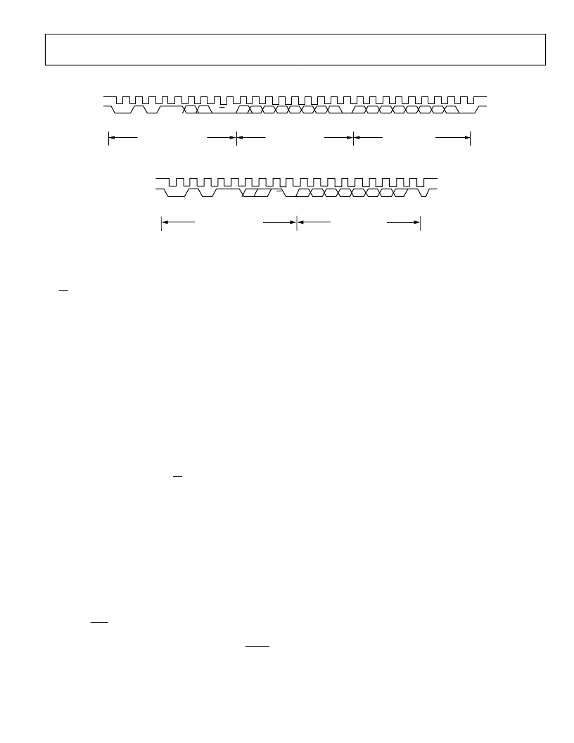
Figure 33. General I
2
C Write Pattern
0
SDA
FRAME1
SLAVE ADDRESS BYTE
FRAME 2
RDAC REGISTER
SCL
ACK.BY
AD525x
NO ACK.BY
MASTER
STOP BY
MASTER
STARTBY
MASTER
0
1
1
0
1
1
AD1 AD0
D7
D6
D5
D4
D3
D2
D1
D0
9
1
9
R/W
Figure 34. General I
2
C Read Pattern
The first byte of the AD5253/AD5254 is a slave address byte
(see Figure 24 and Figure 25). It has a 7-bit slave address and an
R/W bit. The 5 MSB of the slave address are 01011, and the
following 2 LSB are determined by the states of the AD1 and
AD0 pins. AD1 and AD0 allow the user to place up to four
AD5253/AD5254s on one bus. The 2-wire I
2
C serial bus
protocol operates as follows:
AD5253/AD5254 can be controlled via an I
2
C compatible serial
bus, and are connected to this bus as slave device. The 2-wire
I
2
C serial bus protocol follows (see Figure 33 and Figure 34):
1.
The master initiates a data transfer by establishing a start
condition, such that SDA goes from high to low while SCL
is high (Figure 33). The following byte is the slave address
byte, which consists of the 5 MSB of a slave address defined
as 01011. The next two bits are AD1 and AD0, I
2
C device
address bits. Depending on the states of their AD1 and
AD0 bits, four AD5253/AD5254s can be addressed on the
same bus. The last LSB, the R/W bit, determines whether
data is read from or written to the slave device.
The slave whose address corresponds to the transmitted
address responds by pulling the SDA line low during the
ninth clock pulse (this is called an acknowledge bit). At this
stage, all other devices on the bus remain idle while the
selected device waits for data to be written to or read from
its serial register.
2.
In the write mode (except when restoring EEMEM to the
RDAC register), there is an instruction byte that follows the
slave address byte. The MSB of the instruction byte labeled
CMD/REG. MSB = 1 enables CMD, the command
instruction byte; MSB = 0 enables general register writing.
The third MSB in the instruction byte, labeled EE/RDAC, is
true only when MSB = 0 or in general writing mode. EE
enables the EEMEM register and REG enables the RDAC
register. The 5 LSB, A4 to A0, designed the addresses of the
EEMEM and RDAC registers; see Figure 27 and Figure 28.
When MSB = 1 or when in CMD mode, the four bits
following MSB are C3 to C1, which correspond to 12
predefined EEMEM controls and quick commands; there
are also four factory reserved commands. The 3 LSB—A2,
A1, and A0—are 4-channel RDAC addresses (see
Figure 31). After acknowledging the instruction byte, the
last byte in the write mode is the data byte. Data is
transmitted over the serial bus in sequences of nine clock
pulses (eight data bits followed by an acknowledge bit). The
transitions on the SDA line must occur during the low
period of SCL and remain stable during the high period of
SCL (Figure 33).
3.
In current read mode, the RDAC0 data byte immediately
follows the acknowledgment of the slave address byte. After
an acknowledgement, RDAC1 follows, then RDAC2, and so
on (there is a slight difference in write mode, where the last
eight data bits representing RDAC3 data are followed by a
no acknowledge bit). Similarly, the transitions on the SDA
line must occur during the low period of SCL and remain
stable during the high period of SCL (see Figure 34).
Another reading method, random read method, is shown
in Figure 30.
4.
When all data bits have been read or written, a stop
condition is established by the master. A stop condition is
defined as a low-to-high transition on the SDA line while
SCL is high. In write mode, the master pulls the SDA line
high during the 10
th
clock pulse to establish a stop
condition (Figure 33). In read mode, the master issues a no
acknowledge for the ninth clock pulse, i.e., the SDA line
remains high. The master then brings the SDA line low
before the 10
th
clock pulse, which goes high to establish a
stop condition (Figure 34).
相关PDF资料 |
PDF描述 |
|---|---|
| AD5254BRU50 | Dual, 256-Tap, Nonvolatile, I2C-Interface, Digital Potentiometers |
| AD5254BRU50-RL7 | Dual, 256-Tap, Nonvolatile, I2C-Interface, Digital Potentiometers |
| AD5253 | Dual, 256-Tap, Nonvolatile, I2C-Interface, Digital Potentiometers |
| AD5253BRU1 | Dual, 256-Tap, Nonvolatile, I2C-Interface, Digital Potentiometers |
| AD5253BRU1-RL7 | Dual, 256-Tap, Nonvolatile, I2C-Interface, Digital Potentiometers |
相关代理商/技术参数 |
参数描述 |
|---|---|
| AD5254BRU10-RL7 | 功能描述:IC DGTL POT QUAD 10K 20-TSSOP RoHS:否 类别:集成电路 (IC) >> 数据采集 - 数字电位器 系列:- 标准包装:3,000 系列:DPP 接片:32 电阻(欧姆):10k 电路数:1 温度系数:标准值 300 ppm/°C 存储器类型:非易失 接口:3 线串行(芯片选择,递增,增/减) 电源电压:2.5 V ~ 6 V 工作温度:-40°C ~ 85°C 安装类型:表面贴装 封装/外壳:8-WFDFN 裸露焊盘 供应商设备封装:8-TDFN(2x3) 包装:带卷 (TR) |
| AD5254BRU1-RL7 | 功能描述:IC DGTL POT QUAD 1K 20-TSSOP RoHS:否 类别:集成电路 (IC) >> 数据采集 - 数字电位器 系列:- 标准包装:3,000 系列:DPP 接片:32 电阻(欧姆):10k 电路数:1 温度系数:标准值 300 ppm/°C 存储器类型:非易失 接口:3 线串行(芯片选择,递增,增/减) 电源电压:2.5 V ~ 6 V 工作温度:-40°C ~ 85°C 安装类型:表面贴装 封装/外壳:8-WFDFN 裸露焊盘 供应商设备封装:8-TDFN(2x3) 包装:带卷 (TR) |
| AD5254BRU50 | 功能描述:IC DGTL POT QUAD 50K 20-TSSOP RoHS:否 类别:集成电路 (IC) >> 数据采集 - 数字电位器 系列:- 标准包装:3,000 系列:DPP 接片:32 电阻(欧姆):10k 电路数:1 温度系数:标准值 300 ppm/°C 存储器类型:非易失 接口:3 线串行(芯片选择,递增,增/减) 电源电压:2.5 V ~ 6 V 工作温度:-40°C ~ 85°C 安装类型:表面贴装 封装/外壳:8-WFDFN 裸露焊盘 供应商设备封装:8-TDFN(2x3) 包装:带卷 (TR) |
| AD5254BRU50-RL7 | 功能描述:IC DGTL POT QUAD 50K 20-TSSOP RoHS:否 类别:集成电路 (IC) >> 数据采集 - 数字电位器 系列:- 标准包装:3,000 系列:DPP 接片:32 电阻(欧姆):10k 电路数:1 温度系数:标准值 300 ppm/°C 存储器类型:非易失 接口:3 线串行(芯片选择,递增,增/减) 电源电压:2.5 V ~ 6 V 工作温度:-40°C ~ 85°C 安装类型:表面贴装 封装/外壳:8-WFDFN 裸露焊盘 供应商设备封装:8-TDFN(2x3) 包装:带卷 (TR) |
| AD5254BRUZ1 | 功能描述:IC DGTL POT QUAD 1K I2C 20-TSSOP RoHS:是 类别:集成电路 (IC) >> 数据采集 - 数字电位器 系列:- 产品培训模块:Lead (SnPb) Finish for COTS Obsolescence Mitigation Program 标准包装:1 系列:- 接片:256 电阻(欧姆):100k 电路数:1 温度系数:标准值 35 ppm/°C 存储器类型:非易失 接口:3 线串口 电源电压:2.7 V ~ 5.25 V 工作温度:-40°C ~ 85°C 安装类型:表面贴装 封装/外壳:8-WDFN 裸露焊盘 供应商设备封装:8-TDFN-EP(3x3) 包装:剪切带 (CT) 产品目录页面:1399 (CN2011-ZH PDF) 其它名称:MAX5423ETA+TCT |
发布紧急采购,3分钟左右您将得到回复。