- 您现在的位置:买卖IC网 > PDF目录373874 > AD5259 (Analog Devices, Inc.) 18 Bit, 1.25MSPS Single Channel Delta-Sigma ADC Single with FIFO 64-HTQFP -40 to 105 PDF资料下载
参数资料
| 型号: | AD5259 |
| 厂商: | Analog Devices, Inc. |
| 英文描述: | 18 Bit, 1.25MSPS Single Channel Delta-Sigma ADC Single with FIFO 64-HTQFP -40 to 105 |
| 中文描述: | 非易失,I2C兼容256级,数字电位器 |
| 文件页数: | 16/24页 |
| 文件大小: | 1039K |
| 代理商: | AD5259 |
AD5259
I
2
C-COMPATIBLE FORMAT
The following generic, write, read, and store/restore control
registers for the AD5259 all refer to the device addresses listed
in Table 5; the mode/condition reference key (S, P, SA, MA,
NA, W, R, and X) is listed below.
S
= Start Condition
Rev. A | Page 16 of 24
P
= Stop Condition
SA
= Slave Acknowledge
MA
= Master Acknowledge
NA
= No Acknowledge
W
= Write
R
= Read
X
= Don’t Care
AD1 and AD0 are two-state address pins.
Table 5. Device Address Lookup
AD1 Address Pin
AD0 Address Pin
0
0
1
0
0
1
1
1
I
2
C Device Address
0011000
0011010
1001100
1001110
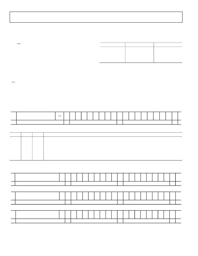
GENERIC INTERFACE
Table 6. Generic Interface Format
7-Bit Device Address
(See Table 5)
Slave Address Byte
S
R/W
SA C2 C1 C0 A4 A3 A2 A1 A0 SA D7 D6 D5 D4 D3 D2 D1 D0 SA P
Instruction Byte
Data Byte
Table 7. RDAC-to-EEPROM Interface Command Descriptions
C2
C1
C0
Command Description
0
0
0
Operation Between Interface and RDAC.
0
0
1
Operation Between Interface and EEPROM.
0
1
0
Operation Between Interface and Write Protection Register. See Table 10.
1
0
0
NOP.
1
0
1
Restore EEPROM to RDAC.
1
1
0
Store RDAC to EEPROM.
WRITE MODES
Table 8. Writing to RDAC Register
7-Bit Device Address
(See Table 5)
Slave Address Byte
S
0
SA 0
0
0
0
0
0
0
0
SA D7 D6 D5 D4 D3 D2 D1 D0 SA P
Data Byte
Instruction Byte
Table 9. Writing to EEPROM Register
7-Bit Device Address
(See Table 5)
Slave Address Byte
S
0
SA 0
0
1
0
0
0
0
0
SA D7 D6 D5 D4 D3 D2 D1 D0 SA P
Data Byte
Instruction Byte
Table 10. Activating/Deactivating Software Write Protect
7-Bit Device Address
(See Table 5)
Slave Address Byte
S
0
SA 0
1
0
0
0
0
0
0
SA 0
0
0
0
0
0
0
WP SA P
Instruction Byte
Data Byte
In order to activate the write protection mode, the WP bit in Table 10 must be logic high. To deactivate the write protection, the
command must be sent again, except with the WP in logic zero state. WP is reset to the deactivated mode if power is cycled off and on.
相关PDF资料 |
PDF描述 |
|---|---|
| AD5259BRMZ5 | Nonvolatile, I2C-Compatible 256-Position, Digital Potentiometer |
| AD5259BRMZ5-R7 | 18 Bit, 1.25MSPS Single Channel Delta-Sigma ADC Single with FIFO 64-HTQFP -40 to 105 |
| AD5259BRMZ50 | Nonvolatile, I2C-Compatible 256-Position, Digital Potentiometer |
| AD5259BRMZ50-R7 | Nonvolatile, I2C-Compatible 256-Position, Digital Potentiometer |
| AD5259BRMZ10 | Nonvolatile, I2C-Compatible 256-Position, Digital Potentiometer |
相关代理商/技术参数 |
参数描述 |
|---|---|
| AD5259BCPZ100-R7 | 功能描述:IC POT DGTL 100K 256POS 10LFCSP RoHS:是 类别:集成电路 (IC) >> 数据采集 - 数字电位器 系列:- 标准包装:3,300 系列:WiperLock™ 接片:257 电阻(欧姆):100k 电路数:1 温度系数:标准值 150 ppm/°C 存储器类型:易失 接口:3 线 SPI(芯片选择) 电源电压:1.8 V ~ 5.5 V 工作温度:-40°C ~ 125°C 安装类型:表面贴装 封装/外壳:8-VDFN 裸露焊盘 供应商设备封装:8-DFN-EP(3x3) 包装:带卷 (TR) |
| AD5259BCPZ10-R7 | 功能描述:IC POT DGTL 10K 256POS 10LFCSP RoHS:是 类别:集成电路 (IC) >> 数据采集 - 数字电位器 系列:- 标准包装:3,000 系列:DPP 接片:32 电阻(欧姆):10k 电路数:1 温度系数:标准值 300 ppm/°C 存储器类型:非易失 接口:3 线串行(芯片选择,递增,增/减) 电源电压:2.5 V ~ 6 V 工作温度:-40°C ~ 85°C 安装类型:表面贴装 封装/外壳:8-WFDFN 裸露焊盘 供应商设备封装:8-TDFN(2x3) 包装:带卷 (TR) |
| AD5259BCPZ50-R7 | 功能描述:IC POT DGTL 50K 256POS 10LFCSP RoHS:是 类别:集成电路 (IC) >> 数据采集 - 数字电位器 系列:- 标准包装:3,000 系列:DPP 接片:32 电阻(欧姆):10k 电路数:1 温度系数:标准值 300 ppm/°C 存储器类型:非易失 接口:3 线串行(芯片选择,递增,增/减) 电源电压:2.5 V ~ 6 V 工作温度:-40°C ~ 85°C 安装类型:表面贴装 封装/外壳:8-WFDFN 裸露焊盘 供应商设备封装:8-TDFN(2x3) 包装:带卷 (TR) |
| AD5259BCPZ5-R7 | 功能描述:IC POT DGTL 5K 256POS 10LFCSP RoHS:是 类别:集成电路 (IC) >> 数据采集 - 数字电位器 系列:- 标准包装:3,000 系列:DPP 接片:32 电阻(欧姆):10k 电路数:1 温度系数:标准值 300 ppm/°C 存储器类型:非易失 接口:3 线串行(芯片选择,递增,增/减) 电源电压:2.5 V ~ 6 V 工作温度:-40°C ~ 85°C 安装类型:表面贴装 封装/外壳:8-WFDFN 裸露焊盘 供应商设备封装:8-TDFN(2x3) 包装:带卷 (TR) |
| AD5259BRMZ10 | 功能描述:IC DGTL POT 10K 256POS 10-MSOP RoHS:是 类别:集成电路 (IC) >> 数据采集 - 数字电位器 系列:- 产品培训模块:Lead (SnPb) Finish for COTS Obsolescence Mitigation Program 标准包装:1 系列:- 接片:256 电阻(欧姆):100k 电路数:1 温度系数:标准值 35 ppm/°C 存储器类型:非易失 接口:3 线串口 电源电压:2.7 V ~ 5.25 V 工作温度:-40°C ~ 85°C 安装类型:表面贴装 封装/外壳:8-WDFN 裸露焊盘 供应商设备封装:8-TDFN-EP(3x3) 包装:剪切带 (CT) 产品目录页面:1399 (CN2011-ZH PDF) 其它名称:MAX5423ETA+TCT |
发布紧急采购,3分钟左右您将得到回复。