- 您现在的位置:买卖IC网 > PDF目录373874 > AD5259BCPZ10-R7 (ANALOG DEVICES INC) Nonvolatile, I2C-Compatible 256-Position, Digital Potentiometer PDF资料下载
参数资料
| 型号: | AD5259BCPZ10-R7 |
| 厂商: | ANALOG DEVICES INC |
| 元件分类: | 数字电位计 |
| 英文描述: | Nonvolatile, I2C-Compatible 256-Position, Digital Potentiometer |
| 中文描述: | 10K DIGITAL POTENTIOMETER, 2-WIRE SERIAL CONTROL INTERFACE, 256 POSITIONS, DSO10 |
| 封装: | 3 X 3 MM, 0.80 MM HEIGHT, LEAD FREE, LFCSP-10 |
| 文件页数: | 19/24页 |
| 文件大小: | 1039K |
| 代理商: | AD5259BCPZ10-R7 |
AD5259
ESD PROTECTION OF DIGITAL PINS AND
RESISTOR TERMINALS
The AD5259 V
DD
, V
LOGIC
, and GND power supplies define the
boundary conditions for proper 3-terminal and digital input
operation. Supply signals present on Terminal A, Terminal B,
and Terminal W that exceed V
DD
or GND are clamped by the
internal forward biased ESD protection diodes (see Figure 42).
Digital Input SCL and Digital Input SDA are clamped by ESD
protection diodes with respect to V
LOGIC
and GND as shown in
Figure 43.
Rev. A | Page 19 of 24
GND
A
W
B
V
DD
0
Figure 42. Maximum Terminal Voltages Set by V
DD
and GND
GND
SCL
SDA
V
LOGIC
0
Figure 43. Maximum Terminal Voltages Set by V
LOGIC
and GND
POWER-UP SEQUENCE
Because the ESD protection diodes limit the voltage compliance
at Terminal A, Terminal B, and Terminal W (see Figure 42), it
is important to power GND/V
DD
/V
LOGIC
before applying any
voltage to Terminal A, Terminal B, and Terminal W; otherwise,
the diode is forward biased, so the V
DD
and V
LOGIC
are powered
unintentionally and may affect the user’s circuit. The ideal power-
up sequence is in the following order: GND, V
DD
, V
LOGIC
, digital
inputs, and then V
A
, V
B
, V
V
A
, V
B
B
, V
W
, and the digital inputs is not important as long as
they are powered after GND/V
DD
/V
LOGIC
.
LAYOUT AND POWER SUPPLY BYPASSING
It is good practice to use compact, minimum lead length layout
design. The leads to the inputs should be as direct as possible
with minimum conductor length. Ground paths should have
low resistance and low inductance.
Similarly, it is also good practice to bypass the power supplies
with quality capacitors for optimum stability. Supply leads to
the device should be bypassed with disc or chip ceramic capaci-
tors of 0.01 μF to 0.1 μF. Low ESR 1 μF to 10 μF tantalum or
electrolytic capacitors should also be applied at the supplies to
minimize any transient disturbance and low frequency ripple
(see Figure 44). The digital ground should also be joined
remotely to the analog ground at one point to minimize the
ground bounce.
V
DD
GND
V
DD
C2
10
μ
F
C1
0.1
μ
F
AD5259
+
0
Figure 44. Power Supply Bypassing
MULTIPLE DEVICES ON ONE BUS
The AD5259 has two configurable address pins, Pin AD0 and
Pin AD1. The state of these two pins is registered upon power-
up and decoded into a corresponding I
2
C-compatible 7-bit
address (see Table 5). This allows up to four devices on the bus
to be written to or read from independently.
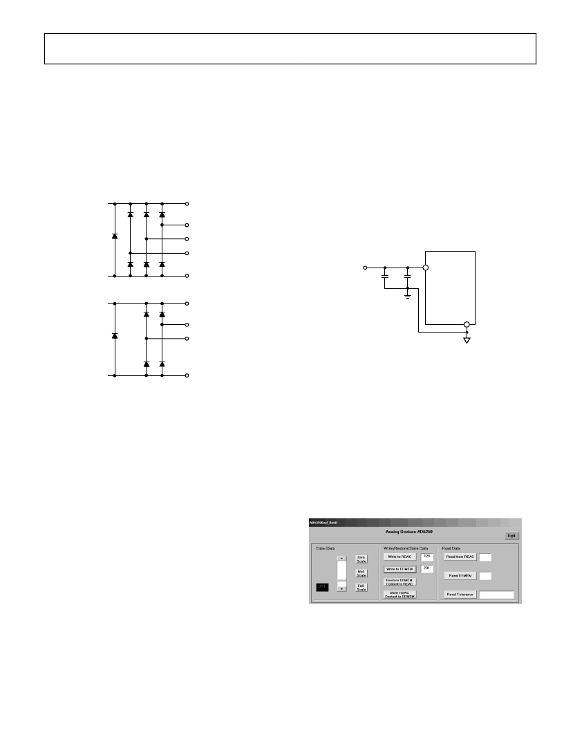
EVALUATION BOARD
An evaluation board, with all necessary software, is available
to program the AD5259 from any PC running Windows 98/
2000/ XP. The graphical user interface, as shown in Figure 45,
is straightforward and easy to use. More detailed information
is available in the board’s user manual.
W
. The relative order of powering
0
Figure 45. AD5259 Evaluation Board Software
相关PDF资料 |
PDF描述 |
|---|---|
| AD5259EVAL2 | Nonvolatile, I2C-Compatible 256-Position, Digital Potentiometer |
| AD5259BCPZ100-R7 | Nonvolatile, I2C-Compatible 256-Position, Digital Potentiometer |
| AD5259 | 18 Bit, 1.25MSPS Single Channel Delta-Sigma ADC Single with FIFO 64-HTQFP -40 to 105 |
| AD5259BRMZ5 | Nonvolatile, I2C-Compatible 256-Position, Digital Potentiometer |
| AD5259BRMZ5-R7 | 18 Bit, 1.25MSPS Single Channel Delta-Sigma ADC Single with FIFO 64-HTQFP -40 to 105 |
相关代理商/技术参数 |
参数描述 |
|---|---|
| AD5259BCPZ50-R7 | 功能描述:IC POT DGTL 50K 256POS 10LFCSP RoHS:是 类别:集成电路 (IC) >> 数据采集 - 数字电位器 系列:- 标准包装:3,000 系列:DPP 接片:32 电阻(欧姆):10k 电路数:1 温度系数:标准值 300 ppm/°C 存储器类型:非易失 接口:3 线串行(芯片选择,递增,增/减) 电源电压:2.5 V ~ 6 V 工作温度:-40°C ~ 85°C 安装类型:表面贴装 封装/外壳:8-WFDFN 裸露焊盘 供应商设备封装:8-TDFN(2x3) 包装:带卷 (TR) |
| AD5259BCPZ5-R7 | 功能描述:IC POT DGTL 5K 256POS 10LFCSP RoHS:是 类别:集成电路 (IC) >> 数据采集 - 数字电位器 系列:- 标准包装:3,000 系列:DPP 接片:32 电阻(欧姆):10k 电路数:1 温度系数:标准值 300 ppm/°C 存储器类型:非易失 接口:3 线串行(芯片选择,递增,增/减) 电源电压:2.5 V ~ 6 V 工作温度:-40°C ~ 85°C 安装类型:表面贴装 封装/外壳:8-WFDFN 裸露焊盘 供应商设备封装:8-TDFN(2x3) 包装:带卷 (TR) |
| AD5259BRMZ10 | 功能描述:IC DGTL POT 10K 256POS 10-MSOP RoHS:是 类别:集成电路 (IC) >> 数据采集 - 数字电位器 系列:- 产品培训模块:Lead (SnPb) Finish for COTS Obsolescence Mitigation Program 标准包装:1 系列:- 接片:256 电阻(欧姆):100k 电路数:1 温度系数:标准值 35 ppm/°C 存储器类型:非易失 接口:3 线串口 电源电压:2.7 V ~ 5.25 V 工作温度:-40°C ~ 85°C 安装类型:表面贴装 封装/外壳:8-WDFN 裸露焊盘 供应商设备封装:8-TDFN-EP(3x3) 包装:剪切带 (CT) 产品目录页面:1399 (CN2011-ZH PDF) 其它名称:MAX5423ETA+TCT |
| AD5259BRMZ100 | 功能描述:IC DGTL POT 100K 256POS 10-MSOP RoHS:是 类别:集成电路 (IC) >> 数据采集 - 数字电位器 系列:- 产品培训模块:Lead (SnPb) Finish for COTS Obsolescence Mitigation Program 标准包装:1 系列:- 接片:256 电阻(欧姆):100k 电路数:1 温度系数:标准值 35 ppm/°C 存储器类型:非易失 接口:3 线串口 电源电压:2.7 V ~ 5.25 V 工作温度:-40°C ~ 85°C 安装类型:表面贴装 封装/外壳:8-WDFN 裸露焊盘 供应商设备封装:8-TDFN-EP(3x3) 包装:剪切带 (CT) 产品目录页面:1399 (CN2011-ZH PDF) 其它名称:MAX5423ETA+TCT |
| AD5259BRMZ100-R7 | 功能描述:IC POT DGTL 100K 256POS 10MSOP RoHS:是 类别:集成电路 (IC) >> 数据采集 - 数字电位器 系列:- 标准包装:3,000 系列:DPP 接片:32 电阻(欧姆):10k 电路数:1 温度系数:标准值 300 ppm/°C 存储器类型:非易失 接口:3 线串行(芯片选择,递增,增/减) 电源电压:2.5 V ~ 6 V 工作温度:-40°C ~ 85°C 安装类型:表面贴装 封装/外壳:8-WFDFN 裸露焊盘 供应商设备封装:8-TDFN(2x3) 包装:带卷 (TR) |
发布紧急采购,3分钟左右您将得到回复。