- 您现在的位置:买卖IC网 > PDF目录9425 > AD5262BRUZ20-RL7 (Analog Devices Inc)IC DGTL POT 256POS 20K 16TSSOP PDF资料下载
参数资料
| 型号: | AD5262BRUZ20-RL7 |
| 厂商: | Analog Devices Inc |
| 文件页数: | 10/24页 |
| 文件大小: | 0K |
| 描述: | IC DGTL POT 256POS 20K 16TSSOP |
| 标准包装: | 1 |
| 接片: | 256 |
| 电阻(欧姆): | 20k |
| 电路数: | 2 |
| 温度系数: | 标准值 35 ppm/°C |
| 存储器类型: | 易失 |
| 接口: | 4 线 SPI(芯片选择) |
| 电源电压: | 4.5 V ~ 16.5 V,±4.5 V ~ 5.5 V |
| 工作温度: | -40°C ~ 85°C |
| 安装类型: | 表面贴装 |
| 封装/外壳: | 16-TSSOP(0.173",4.40mm 宽) |
| 供应商设备封装: | 16-TSSOP |
| 包装: | 标准包装 |
| 其它名称: | AD5262BRUZ20-RL7DKR |
AD5260/AD5262
Rev. A | Page 18 of 24
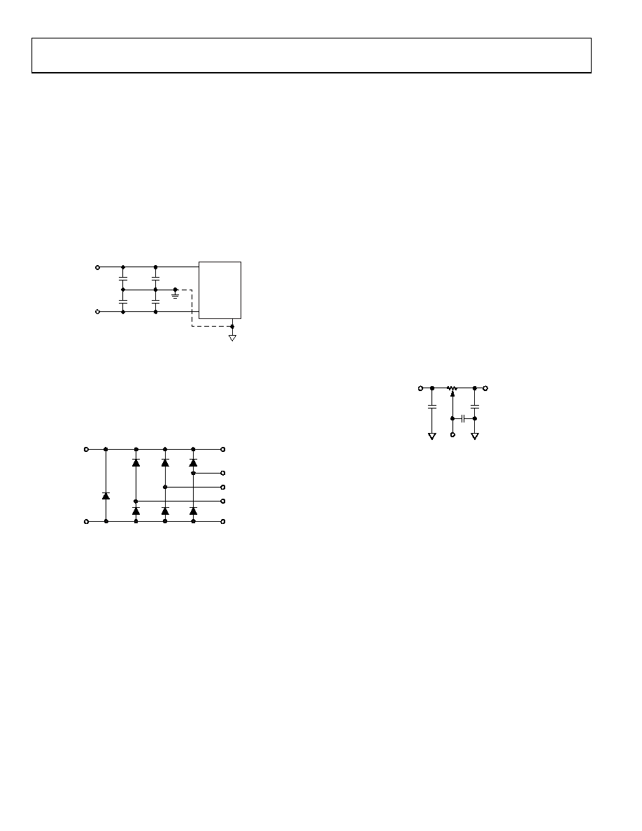
LAYOUT AND POWER SUPPLY BYPASSING
It is good practice to employ a compact, minimum lead length
layout design. The leads to the input should be as direct as
possible with a minimum conductor length. Ground paths
should have low resistance and low inductance.
Similarly, it is also good practice to bypass the power supplies
with quality capacitors for optimum stability. Supply leads to
the device should be bypassed with 0.01 μF to 0.1 μF disc or
chip ceramic capacitors. Low ESR 1 μF to 10 μF tantalum or
electrolytic capacitors should also be applied at the supplies to
minimize any transient disturbance (see Figure 55). Note that
the digital ground should also be joined remotely to the analog
ground to minimize the ground bounce.
VSS
VDD
VSS
VDD
C3
C4
C1
C2
10F
GND
0.1F
+
026
95-
053
Figure 55. Power Supply Bypassing
TERMINAL VOLTAGE OPERATING RANGE
The AD5260/AD5262 positive VDD and negative VSS power
supply defines the boundary conditions for proper 3-terminal
digital potentiometer operation. Supply signals present on the
A, B, and W terminals that exceed VDD or VSS are clamped by
the internal forward-biased diodes (see Figure 56).
VDD
VSS
A
W
B
02
695-
0
54
Figure 56. Maximum Terminal Voltages Set by VDD and VSS
The ground pin of the AD5260/AD5262 device is primarily
used as a digital ground reference, which needs to be tied to the
common ground of the PCB. The digital input control signals to
the AD5260/AD5262 must be referenced to the device ground
pin (GND), and must satisfy the logic level defined in Table 1.
An internal level shift circuit ensures that the common-mode
voltage range of the three terminals extends from VSS to VDD
regardless of the digital input level.
POWER-UP SEQUENCE
Because there are diodes to limit the voltage compliance at
Terminal A, Terminal B, and Terminal W (see Figure 56), it is
important to power VDD/VSS first before applying any voltage to
the A, B, and W terminals. Otherwise, the diode becomes forward
biased such that VDD/VSS are powered unintentionally and may
affect the rest of the user’s circuit. The ideal power-up sequence
is in the following order: GND, VDD, VSS, VL, the digital inputs,
and VA/VB/VW. The order of powering VA/VB/VW and the digital
inputs is not important as long as they are powered after VDD/VSS.
RDAC CIRCUIT SIMULATION MODEL
The internal parasitic capacitances and the external capacitive
loads dominate the ac characteristics of the RDACs. Configured
as a potentiometer divider, the 3 dB bandwidth of the AD5260
(20 kΩ resistor) measures 310 kHz at half scale. Figure 28 provides
the large signal Bode plot characteristics of the three available
resistor versions 20 kΩ, 50 kΩ, and 200 kΩ. A parasitic simula-
tion model is shown in Figure 57. The following section provides a
macro model net list for the 20 kΩ RDAC.
AB
55pF
CB
25pF
CA
25pF
CW
RDAC
20k
W
02
695
-071
Figure 57. RDAC Circuit Simulation Model for RDAC 20 kΩ
MACRO MODEL NET LIST FOR RDAC
PARAM D=256, RDAC=20E3
*
SUBCKT DPOT (A,W,B)
*
CA
A
0
25E-12
RWA
A
W
{(1-D/256)*RDAC+60}
CW
W
0
55E-12
RWB
W
B
{D/256*RDAC+60}
CB
B
0
25E-12
*
.ENDS DPOT
相关PDF资料 |
PDF描述 |
|---|---|
| AD5282BRUZ50 | IC DUAL POT 50K 256POS 16-TSSOP |
| AD5262BRUZ200 | IC POT DUAL 200K 256POS 16TSSOP |
| AD5262BRUZ50 | IC POT DUAL 50K 256POS 16TSSOP |
| AD5262BRUZ20 | IC POT DUAL 20K 256POS 16TSSOP |
| 74LCX138M | DECODER/DEMUX 1OF8 5V 16-SOIC |
相关代理商/技术参数 |
参数描述 |
|---|---|
| AD5262BRUZ50 | 功能描述:IC POT DUAL 50K 256POS 16TSSOP RoHS:是 类别:集成电路 (IC) >> 数据采集 - 数字电位器 系列:- 产品培训模块:Lead (SnPb) Finish for COTS Obsolescence Mitigation Program 标准包装:1 系列:- 接片:256 电阻(欧姆):100k 电路数:1 温度系数:标准值 35 ppm/°C 存储器类型:非易失 接口:3 线串口 电源电压:2.7 V ~ 5.25 V 工作温度:-40°C ~ 85°C 安装类型:表面贴装 封装/外壳:8-WDFN 裸露焊盘 供应商设备封装:8-TDFN-EP(3x3) 包装:剪切带 (CT) 产品目录页面:1399 (CN2011-ZH PDF) 其它名称:MAX5423ETA+TCT |
| AD5262BRUZ50 | 制造商:Analog Devices 功能描述:IC DIGITAL POT 50KOHM 256 DUAL 16-TSSO |
| AD5262BRUZ50-RL7 | 功能描述:IC POT DUAL 50K 256POS 16TSSOP RoHS:是 类别:集成电路 (IC) >> 数据采集 - 数字电位器 系列:- 标准包装:3,000 系列:DPP 接片:32 电阻(欧姆):10k 电路数:1 温度系数:标准值 300 ppm/°C 存储器类型:非易失 接口:3 线串行(芯片选择,递增,增/减) 电源电压:2.5 V ~ 6 V 工作温度:-40°C ~ 85°C 安装类型:表面贴装 封装/外壳:8-WFDFN 裸露焊盘 供应商设备封装:8-TDFN(2x3) 包装:带卷 (TR) |
| AD5262-EVAL | 制造商:Analog Devices 功能描述:EVAL KIT FOR 1-/2CH 15 V DGTL POTENTIOMETERS - Bulk |
| AD5263 | 制造商:AD 制造商全称:Analog Devices 功能描述:Preliminary Technical Data |
发布紧急采购,3分钟左右您将得到回复。