- 您现在的位置:买卖IC网 > PDF目录373875 > AD5273EVAL (Analog Devices, Inc.) 64-Position OTP Digital Potentiometer PDF资料下载
参数资料
| 型号: | AD5273EVAL |
| 厂商: | Analog Devices, Inc. |
| 元件分类: | 数字电位计 |
| 英文描述: | 64-Position OTP Digital Potentiometer |
| 中文描述: | 64工位检察官数字电位器 |
| 文件页数: | 12/20页 |
| 文件大小: | 987K |
| 代理商: | AD5273EVAL |
AD5273
–12–
Note that in the zero-scale condition a finite wiper resistance of
60 is present. Care should be taken to limit the current flow
between W and B in this state to a maximum pulse current of no
more than 20 mA. Otherwise, degradation or possible destruction
of the internal switch contact can occur.
Similar to the mechanical potentiometer, the resistance of the
RDAC between the wiper W and terminal A also produces a
digitally controlled complementary resistance R
WA
. When these
terminals are used, terminal B can be opened. Setting the resis-
tance value for R
WA
starts at a maximum value of resistance and
decreases as the data loaded in the latch increases in value. The
general equation for this operation is:
D
R
R
WA
AB
( )
=
63
R
D
W
¥
+
63
–
(2)
For
R
AB
= 10 k and terminal B is opened, the following output
resistance
R
WA
will be set for the following RDAC latch codes.
D (DEC)
63
32
1
0
R
WA
( ) Output State
60 Full-Scale
4980 Midscale
9901 1 LSB
10060 Zero-Scale
The typical distribution of the nominal resistance R
AB
from channel
to channel matches within ±1%. Device-to-device matching is
process lot dependent and is possible to have ±30% variation.
D5
D4
D3
D2
D1
D0
RDAC
LATCH
AND
DECODER
R
S
R
S
R
S
A
W
B
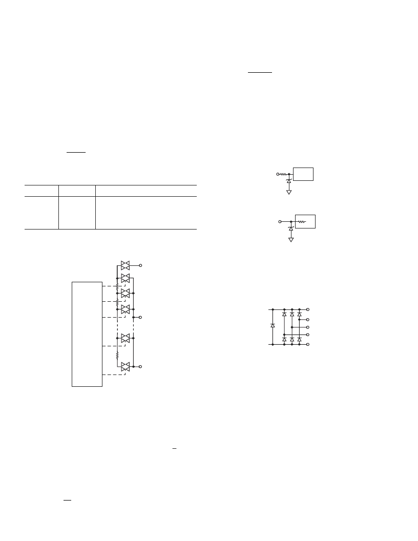
Figure 3. Equivalent RDAC Circuit
Voltage Output Operation
Similar to the D/A converter, the digital potentiometer easily
generates a voltage divider at wiper-to-B and wiper-to-A to be
proportional to the input voltage at A–B. Unlike the polarity of
V
DD
, which must be positive, voltage across A–B, W–A, and W–B
can be at either polarity as long as the voltage across them
is <
I
V
DD
I
.
If ignoring the effect of the wiper resistance for approximation,
connecting terminal A to 5 V and terminal B to ground produces
an output voltage at the wiper-to-B starting at 0 V up to 5 V.
Each
LSB of voltage is equal to the voltage applied across terminal A–B,
divided by the 63 position of the potentiometer divider as:
DV
W
A
( )
=
63
(3)
V
D
For a more accurate calculation, which includes the effect of
wiper resistance,
V
W
can be found as:
R
D
R
AB
(4)
Operation of the digital potentiometer in the divider mode results
in a more accurate operation overtemperature. Unlike the rheostat
mode, the output voltage is dependent mainly on the ratio of the
internal resistors
R
WA
and
R
WB
and not the absolute values, there-
fore, the temperature drift reduces to 10 ppm/°C.
V
D
( )
=
V
W
WB
A
( )
ESD PROTECTION
All digital inputs are protected with a series input resistor and
parallel Zener ESD structures shown in Figures 4a and 4b. This
applies to digital input pins SDA and SCL.
LOGIC
340
Figure 4a. ESD Protection of Digital Pins
A,B,W
Figure 4b. ESD Protection of Resistor Terminals
TERMINAL VOLTAGE OPERATING RANGE
The V
DD
of AD5273 defines the boundary conditions for proper
3-terminal digital potentiometer operation. Supply signals present
on terminals A, B, and W that exceed V
DD
will be clamped by the
internal forward-biased diodes. See Figure 5.
GND
A
W
B
V
DD
Figure 5. Maximum Terminal Voltages Set by V
DD
POWER-UP SEQUENCE
Since there are ESD protection diodes that limit the voltage compli-
ance at terminals A, B, and W (Figure 5), it is important to power
V
DD
first before applying any voltage to terminals A, B, and W.
Otherwise, the diode will be forward-biased such that V
DD
will
be powered unintentionally and may affect the rest of the users’
circuits. The ideal power-up sequence is in the following order:
GND, V
DD
, digital inputs, and V
A/B/W
. The order of powering V
A
,
V
B
, V
W
, and digital inputs is not important as long as they are
powered after V
DD
.
POWER SUPPLY CONSIDERATIONS
AD5273 employs fuse link technology, which requires an adequate
current density to blow the internal fuses to achieve a given setting.
As a result, the power supply, either an on-board linear regulator
or rack-mount power supply, must be rated at 5 V with less than
±5% tolerance. The supply should be able to handle 100 mA of
transient current, and lasts about 400 ms, during the one-time
programming. A low ESR 1 μF to 10 μF tantalum or electrolytic
REV. 0
相关PDF资料 |
PDF描述 |
|---|---|
| AD5282BRU50 | 32-Tap. Nonvolatile. Linear-Taper Digital Potentiometers in SOT23 |
| AD5280 | CONNECTOR ACCESSORY |
| AD5280BRU50 | 32-Tap. Nonvolatile. Linear-Taper Digital Potentiometers in SOT23 |
| AD5280BRU20 | Low Power, 8 Channel, 10-bit, 40MSPS ADC, 1.8V 257-BGA MICROSTAR -40 to 85 |
| AD5280BRU200 | 32-Tap. Nonvolatile. Linear-Taper Digital Potentiometers in SOT23 |
相关代理商/技术参数 |
参数描述 |
|---|---|
| AD5274 | 制造商:AD 制造商全称:Analog Devices 功能描述:1024-/256-Position, 1% Resistor Tolerance Error, I2C Interface and 50-TP Memory Digital Rheostat |
| AD5274BCPZ-100-RL7 | 功能描述:IC RHEOSTAT 5V 50-TP 256 10MSOP RoHS:是 类别:集成电路 (IC) >> 数据采集 - 数字电位器 系列:- 标准包装:3,000 系列:DPP 接片:32 电阻(欧姆):10k 电路数:1 温度系数:标准值 300 ppm/°C 存储器类型:非易失 接口:3 线串行(芯片选择,递增,增/减) 电源电压:2.5 V ~ 6 V 工作温度:-40°C ~ 85°C 安装类型:表面贴装 封装/外壳:8-WFDFN 裸露焊盘 供应商设备封装:8-TDFN(2x3) 包装:带卷 (TR) |
| AD5274BCPZ-20-RL7 | 功能描述:IC RHEOSTAT 5V 50-TP 256 10MSOP RoHS:是 类别:集成电路 (IC) >> 数据采集 - 数字电位器 系列:- 标准包装:3,000 系列:DPP 接片:32 电阻(欧姆):10k 电路数:1 温度系数:标准值 300 ppm/°C 存储器类型:非易失 接口:3 线串行(芯片选择,递增,增/减) 电源电压:2.5 V ~ 6 V 工作温度:-40°C ~ 85°C 安装类型:表面贴装 封装/外壳:8-WFDFN 裸露焊盘 供应商设备封装:8-TDFN(2x3) 包装:带卷 (TR) |
| AD5274BRMZ-100 | 功能描述:IC RHEOSTAT 5V 50TP 256 10MSOP RoHS:是 类别:集成电路 (IC) >> 数据采集 - 数字电位器 系列:- 产品培训模块:Lead (SnPb) Finish for COTS Obsolescence Mitigation Program 标准包装:1 系列:- 接片:256 电阻(欧姆):100k 电路数:1 温度系数:标准值 35 ppm/°C 存储器类型:非易失 接口:3 线串口 电源电压:2.7 V ~ 5.25 V 工作温度:-40°C ~ 85°C 安装类型:表面贴装 封装/外壳:8-WDFN 裸露焊盘 供应商设备封装:8-TDFN-EP(3x3) 包装:剪切带 (CT) 产品目录页面:1399 (CN2011-ZH PDF) 其它名称:MAX5423ETA+TCT |
| AD5274BRMZ-100-RL7 | 功能描述:IC RHEOSTAT 5V 50-TP 256 10MSOP RoHS:是 类别:集成电路 (IC) >> 数据采集 - 数字电位器 系列:- 标准包装:3,000 系列:DPP 接片:32 电阻(欧姆):10k 电路数:1 温度系数:标准值 300 ppm/°C 存储器类型:非易失 接口:3 线串行(芯片选择,递增,增/减) 电源电压:2.5 V ~ 6 V 工作温度:-40°C ~ 85°C 安装类型:表面贴装 封装/外壳:8-WFDFN 裸露焊盘 供应商设备封装:8-TDFN(2x3) 包装:带卷 (TR) |
发布紧急采购,3分钟左右您将得到回复。