- 您现在的位置:买卖IC网 > PDF目录9288 > AD5282BRU200-REEL7 (Analog Devices Inc)IC DGTL POT DUAL 256POS 16-TSSOP PDF资料下载
参数资料
| 型号: | AD5282BRU200-REEL7 |
| 厂商: | Analog Devices Inc |
| 文件页数: | 9/28页 |
| 文件大小: | 0K |
| 描述: | IC DGTL POT DUAL 256POS 16-TSSOP |
| 标准包装: | 1,000 |
| 接片: | 256 |
| 电阻(欧姆): | 200k |
| 电路数: | 2 |
| 温度系数: | 标准值 30 ppm/°C |
| 存储器类型: | 易失 |
| 接口: | I²C(设备位址) |
| 电源电压: | 4.5 V ~ 16.5 V,±4.5 V ~ 5.5 V |
| 工作温度: | -40°C ~ 85°C |
| 安装类型: | 表面贴装 |
| 封装/外壳: | 16-TSSOP(0.173",4.40mm 宽) |
| 供应商设备封装: | 16-TSSOP |
| 包装: | 带卷 (TR) |
| 其它名称: | AD5282BRU200REEL7 |
第1页第2页第3页第4页第5页第6页第7页第8页当前第9页第10页第11页第12页第13页第14页第15页第16页第17页第18页第19页第20页第21页第22页第23页第24页第25页第26页第27页第28页
AD5280/AD5282
Rev. C | Page 17 of
28
READBACK RDAC VALUE
The AD5280/AD5282 allow the user to read back the RDAC
values in read mode. However, for the dual-channel AD5282,
the channel of interest is the one that is previously selected in
the write mode. When users need to read the RDAC values of
both channels in the AD5282, they can program the first
subaddress in write mode and then change to read mode to read
the first channel value. After that, they can change back to write
mode with the second subaddress and read the second channel
value in read mode again. It is not necessary for users to issue
the Frame 3 data byte in write mode for subsequent readback
programming format.
ADDITIONAL PROGRAMMABLE LOGIC OUTPUT
The AD5280/AD5282 feature additional programmable logic
outputs, O1 and O2, which can be used to drive a digital load,
analog switches, and logic gates. O1 and O2 default to Logic 0. The
logic states of O1 and O2 can be programmed in Frame 2 under
write mode (see Figure 45). These logic outputs have adequate
current driving capability to sink/source milliamperes of load.
Users can also activate O1 and O2 in three ways without
affecting the wiper settings by programming as follows:
Perform start, slave address, acknowledge, and instruction
bytes with O1 and O2 specified, acknowledge, stop.
Complete the write cycle with stop, then start, slave address
byte, acknowledge, instruction byte with O1 and O2
specified, acknowledge, stop.
Not complete the write cycle by not issuing the stop, then
start, slave address byte, acknowledge, instruction byte
with O1 and O2 specified, acknowledge, stop.
SELF-CONTAINED SHUTDOWN FUNCTION AND
PROGRAMMABLE PRESET
Shutdown can be activated by strobing the SHDN pin or
programming the SD bit in the write mode instruction byte.
As shown in
, when shutdown is asserted, the
AD5280/AD5282 open SWA to let the A terminal float and
short the W terminal to the B terminal. The AD5280/AD5282
consume negligible power during shutdown mode, resuming
the previous setting once the
SHDN pin is released.
In addition, shutdown can be implemented with the device
digital output as shown in Figure 47. In this configuration, the
device is shut down during power-up, but the user is allowed to
program the device at any preset levels. When it is done, the
user programs O1 high with the valid coding and the device
exits from shutdown and responds to the new setting. This self-
contained shutdown function allows absolute shutdown during
power-up, which is crucial in hazardous environments, without
adding extra components. Also, the sleep mode programming
feature during shutdown allows the AD5280/AD5282 to have a
programmable preset at any level, a solution that can be as
effective as using other high cost EEPROM devices. Because of
the extra power drawn on RPD, note that a high value should be
chosen for the RPD.
SDA
SHDN
SCL
RPD
O1
02
92
9-
0
46
Figure 47. Shutdown by Internal Logic Output
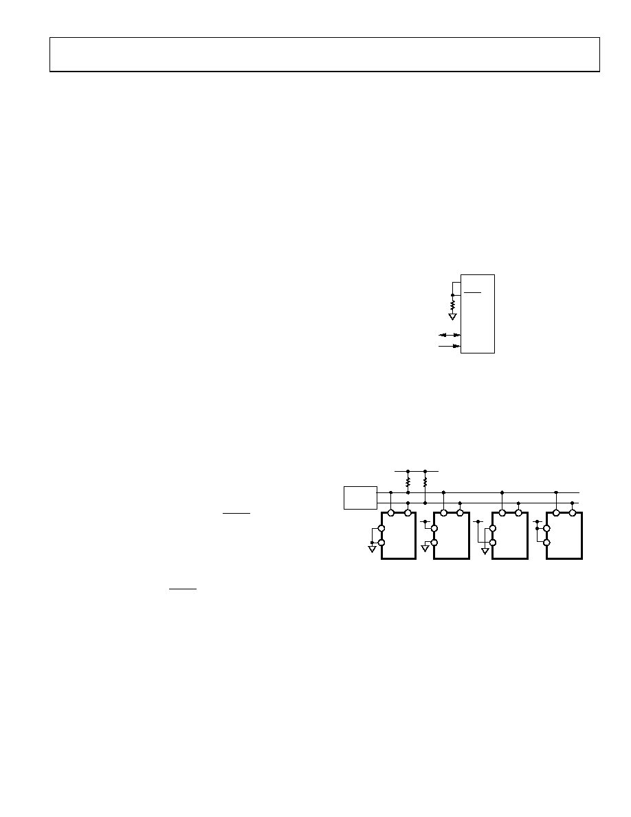
MULTIPLE DEVICES ON ONE BUS
Figure 48 shows four AD5282 devices on the same serial bus.
Each has a different slave address because the states of their Pin
AD0 and Pin AD1 are different. This allows each RDAC within
each device to be written to or read from independently. The
master device output bus line drivers are open-drain pull-
downs in a fully I2C-compatible interface.
SDA
SCL
RP
5V
MASTER
5V
SDA
AD1
AD0
AD5282
SCL
SDA
AD1
AD0
AD5282
SCL
SDA
AD1
AD0
AD5282
SCL
SDA
AD1
AD0
AD5282
SCL
02929-
047
Figure 48. Multiple AD5282 Devices on One Bus
相关PDF资料 |
PDF描述 |
|---|---|
| M83723/85R14077 | CONN RCPT 7POS JAM NUT W/PINS |
| VI-B4Y-MX-F4 | CONVERTER MOD DC/DC 3.3V 49.5W |
| MS3450W24-28PZ | CONN RCPT 24POS WALL MNT W/PINS |
| VI-B6H-IU-F2 | CONVERTER MOD DC/DC 52V 200W |
| VI-26P-MY-F3 | CONVERTER MOD DC/DC 13.8V 50W |
相关代理商/技术参数 |
参数描述 |
|---|---|
| AD5282BRU20-REEL7 | 制造商:Analog Devices 功能描述:DGTL POTENTIOMETER 256POS 20KOHM DUAL 16TSSOP - Tape and Reel |
| AD5282BRU20Z | 制造商:Analog Devices 功能描述:DIG POT 2CH 256 20KOHM 14TSSOP 制造商:Analog Devices 功能描述:DIG POT, 2CH, 256, 20KOHM, TSSOP-16 制造商:Analog Devices 功能描述:DIG POT, 2CH, 256, 20KOHM, 14TSSOP 制造商:Analog Devices 功能描述:DIG POT, 2CH, 256, 20KOHM, 14TSSOP, End To End Resistance:20kohm, Track Taper:Li 制造商:Analog Devices 功能描述:DIG POT, 2CH, 256, 20KOHM, 14TSSOP, End To End Resistance:20kohm, Track Taper:Linear, Resistance Tolerance: 30%, Supply Voltage Min:4.5V, Supply Voltage Max:16.5V, Potentiometer IC Case Style:TSSOP, No. of Pins:16, No. of Steps:256, , RoHS Compliant: Yes |
| AD5282BRU50 | 功能描述:IC DUAL POT 50K 256POS 16-TSSOP RoHS:否 类别:集成电路 (IC) >> 数据采集 - 数字电位器 系列:- 标准包装:3,000 系列:DPP 接片:32 电阻(欧姆):10k 电路数:1 温度系数:标准值 300 ppm/°C 存储器类型:非易失 接口:3 线串行(芯片选择,递增,增/减) 电源电压:2.5 V ~ 6 V 工作温度:-40°C ~ 85°C 安装类型:表面贴装 封装/外壳:8-WFDFN 裸露焊盘 供应商设备封装:8-TDFN(2x3) 包装:带卷 (TR) |
| AD5282BRU50-REEL7 | 功能描述:IC DGTL POT DUAL 256POS 16-TSSOP RoHS:否 类别:集成电路 (IC) >> 数据采集 - 数字电位器 系列:- 标准包装:3,000 系列:DPP 接片:32 电阻(欧姆):10k 电路数:1 温度系数:标准值 300 ppm/°C 存储器类型:非易失 接口:3 线串行(芯片选择,递增,增/减) 电源电压:2.5 V ~ 6 V 工作温度:-40°C ~ 85°C 安装类型:表面贴装 封装/外壳:8-WFDFN 裸露焊盘 供应商设备封装:8-TDFN(2x3) 包装:带卷 (TR) |
| AD5282BRUZ20 | 功能描述:IC DUAL POT 20K 256POS 16-TSSOP RoHS:是 类别:集成电路 (IC) >> 数据采集 - 数字电位器 系列:- 产品培训模块:Lead (SnPb) Finish for COTS Obsolescence Mitigation Program 标准包装:1 系列:- 接片:256 电阻(欧姆):100k 电路数:1 温度系数:标准值 35 ppm/°C 存储器类型:非易失 接口:3 线串口 电源电压:2.7 V ~ 5.25 V 工作温度:-40°C ~ 85°C 安装类型:表面贴装 封装/外壳:8-WDFN 裸露焊盘 供应商设备封装:8-TDFN-EP(3x3) 包装:剪切带 (CT) 产品目录页面:1399 (CN2011-ZH PDF) 其它名称:MAX5423ETA+TCT |
发布紧急采购,3分钟左右您将得到回复。