- 您现在的位置:买卖IC网 > PDF目录9285 > AD5292BRUZ-100-RL7 (Analog Devices Inc)IC DGTL POT 1024POS 20K 14TSSOP PDF资料下载
参数资料
| 型号: | AD5292BRUZ-100-RL7 |
| 厂商: | Analog Devices Inc |
| 文件页数: | 18/32页 |
| 文件大小: | 0K |
| 描述: | IC DGTL POT 1024POS 20K 14TSSOP |
| 设计资源: | Variable Gain Noninverting Amplifier Using AD5292 and OP184 (CN0112) Variable Gain Inverting Amplifier Using AD5292 and OP184 (CN0113) Low Cost, High Voltage, Programmable Gain Instrumentation Amplifier Using AD5292 and AD8221 (CN0114) Programmable High Voltage Source with Boosted Output Current Using AD5292, OP184, and MOSFETs (CN0115) Programmable Bidirectional Current Source Using AD5292 and ADA4091-4 (CN0117) Logarithmic Audio Volume Control with Glitch Reduction Using AD5292 (CN0120) |
| 标准包装: | 1,000 |
| 接片: | 1024 |
| 电阻(欧姆): | 100k |
| 电路数: | 1 |
| 温度系数: | 标准值 35 ppm/°C |
| 存储器类型: | 非易失 |
| 接口: | 4 线串行 |
| 电源电压: | 9 V ~ 33 V,±9 V ~ 16.5 V |
| 工作温度: | -40°C ~ 105°C |
| 安装类型: | 表面贴装 |
| 封装/外壳: | 14-TSSOP(0.173",4.40mm 宽) |
| 供应商设备封装: | 14-TSSOP |
| 包装: | 带卷 (TR) |
第1页第2页第3页第4页第5页第6页第7页第8页第9页第10页第11页第12页第13页第14页第15页第16页第17页当前第18页第19页第20页第21页第22页第23页第24页第25页第26页第27页第28页第29页第30页第31页第32页
AD5291/AD5292
Rev. D | Page 25 of 32
RESISTOR PERFORMANCE MODE
This mode activates a new, patented 1% end-to-end resistor
tolerance that ensures a ±1% resistor tolerance on each code,
(AD5291) or Table 5 (AD5292) to check which codes achieve
±1% resistor tolerance. The resistor performance mode is
activated by programming Bit C2 of the control register (see
Table 13 and Table 14). The typical settling time is shown in
RESET
A low-to-high transition of the hardware RESET pin loads the
RDAC register with the contents of the most recently programmed
20-TP memory location. The AD5291 and AD5292 can also be
reset through software by executing Command 4 (see
).
If no 20-TP memory location is programmed, then the RDAC
register loads with midscale upon reset. The control register is
restored with default bits; see
.
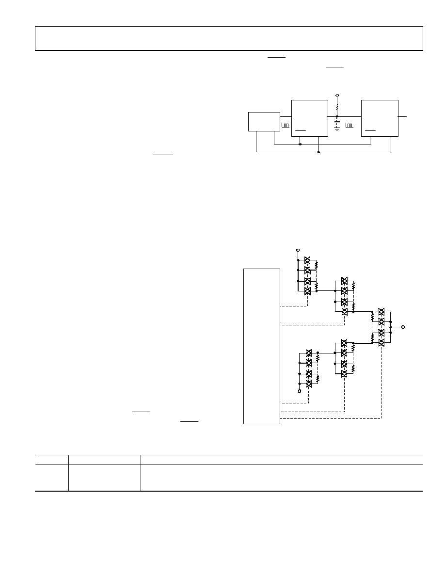
SDO PIN AND DAISY-CHAIN OPERATION
The serial data output pin (SDO) serves two purposes: it can be
used to read the contents of the wiper setting, 50-TP values and
control register using Command 2, Command 5 and Command 7,
respectively (see Table 11) or the SDO pin can be used in daisy-
chain mode. Data is clocked out of SDO on the rising edge of
SCLK. The SDO pin contains an open-drain N-channel FET
that requires a pull-up resistor if this pin is used. To place the
pin in high impedance and minimize the power dissipation
when the pin is used, the 0x8001 data word followed by
Command 0 should be sent to the part. Table 17 provides a
sample listing for the sequence of the serial data input (DIN).
Daisy chaining minimizes the number of port pins required
from the controlling IC. As shown in Figure 64, users need to
tie the SDO pin of one package to the DIN pin of the next
package. Users may need to increase the clock period, because
the pull-up resistor and the capacitive loading at the SDO-to-
DIN interface may require additional time delay between
subsequent devices.
When two AD5291 and AD5292 devices are daisy-chained, 32
bits of data are required. The first 16 bits go to U2, and the
second 16 bits go to U1. Hold the SYNC pin low until all 32 bits
are clocked into their respective shift registers. The SYNC pin is
then pulled high to complete the operation.
Keep the SYNC pin low until all 32 bits are clocked into their
respective serial registers. The SYNC pin is then pulled high to
complete the operation.
DIN
SDO
SCLK
RP
2.2k
DIN
SDO
U1
U2
AD5291/
AD5292
AD5291/
AD5292
SYNC
VLOGIC
MICRO-
CONTROLLER
SCLK
SS
MOSI
SYNC
07
674
-05
0
Figure 64. Daisy-Chain Configuration Using SDO
RDAC ARCHITECTURE
To achieve optimum performance, Analog Devices has patented
the RDAC segmentation architecture for all the digital
potentiometers. In particular, the AD5291 and AD5292 employ
a three-stage segmentation approach, as shown in Figure 65.
The AD5291 and AD5292 wiper switches are designed with the
transmission gate CMOS topology and with the gate voltages
derived from VDD and VSS.
RW
SW
W
RW
8-/10-BIT
ADDRESS
DECODER
A
RL
RM
B
RM
RL
07
67
4
-05
1
Figure 65. Simplified RDAC Circuit
Table 17. Minimize Power Dissipation at SDO Pin
DIN
Action
0xXXXX
Last user command sent to the digipot
0x8001
0xXXXX
Prepares the SDO pin to be placed in high impedance mode
0x0000
High impedance
The SDO pin is placed in high impedance
1 X is don’t care.
相关PDF资料 |
PDF描述 |
|---|---|
| AD5292BRUZ-20-RL7 | IC POT DIG 1024P SPI 20K 14TSSOP |
| DS1100U-200/T&R | IC DELAY LINE 5TAP 200NS 8-USOP |
| VI-274-MW | CONVERTER MOD DC/DC 48V 100W |
| AD7376ARWZ10-RL | IC POT DIGITAL 10K 16-SOIC |
| DS1100U-30/T&R | IC DELAY LINE 5TAP 30NS 8-USOP |
相关代理商/技术参数 |
参数描述 |
|---|---|
| AD5292BRUZ-20 | 功能描述:IC POT DIG 1024P SPI 20K 14TSSOP RoHS:是 类别:集成电路 (IC) >> 数据采集 - 数字电位器 系列:- 产品培训模块:Lead (SnPb) Finish for COTS Obsolescence Mitigation Program 标准包装:1 系列:- 接片:256 电阻(欧姆):100k 电路数:1 温度系数:标准值 35 ppm/°C 存储器类型:非易失 接口:3 线串口 电源电压:2.7 V ~ 5.25 V 工作温度:-40°C ~ 85°C 安装类型:表面贴装 封装/外壳:8-WDFN 裸露焊盘 供应商设备封装:8-TDFN-EP(3x3) 包装:剪切带 (CT) 产品目录页面:1399 (CN2011-ZH PDF) 其它名称:MAX5423ETA+TCT |
| AD5292BRUZ-20-RL7 | 功能描述:IC POT DIG 1024P SPI 20K 14TSSOP RoHS:是 类别:集成电路 (IC) >> 数据采集 - 数字电位器 系列:- 标准包装:3,000 系列:DPP 接片:32 电阻(欧姆):10k 电路数:1 温度系数:标准值 300 ppm/°C 存储器类型:非易失 接口:3 线串行(芯片选择,递增,增/减) 电源电压:2.5 V ~ 6 V 工作温度:-40°C ~ 85°C 安装类型:表面贴装 封装/外壳:8-WFDFN 裸露焊盘 供应商设备封装:8-TDFN(2x3) 包装:带卷 (TR) |
| AD5292BRUZ-50 | 功能描述:IC DGTL POT 1024POS 20K 14TSSOP RoHS:是 类别:集成电路 (IC) >> 数据采集 - 数字电位器 系列:- 产品培训模块:Lead (SnPb) Finish for COTS Obsolescence Mitigation Program 标准包装:1 系列:- 接片:256 电阻(欧姆):100k 电路数:1 温度系数:标准值 35 ppm/°C 存储器类型:非易失 接口:3 线串口 电源电压:2.7 V ~ 5.25 V 工作温度:-40°C ~ 85°C 安装类型:表面贴装 封装/外壳:8-WDFN 裸露焊盘 供应商设备封装:8-TDFN-EP(3x3) 包装:剪切带 (CT) 产品目录页面:1399 (CN2011-ZH PDF) 其它名称:MAX5423ETA+TCT |
| AD5292BRUZ-50-RL7 | 功能描述:IC DGTL POT 1024POS 20K 14TSSOP RoHS:是 类别:集成电路 (IC) >> 数据采集 - 数字电位器 系列:- 标准包装:3,000 系列:DPP 接片:32 电阻(欧姆):10k 电路数:1 温度系数:标准值 300 ppm/°C 存储器类型:非易失 接口:3 线串行(芯片选择,递增,增/减) 电源电压:2.5 V ~ 6 V 工作温度:-40°C ~ 85°C 安装类型:表面贴装 封装/外壳:8-WFDFN 裸露焊盘 供应商设备封装:8-TDFN(2x3) 包装:带卷 (TR) |
| AD5292SRU-20-EP | 制造商:Analog Devices 功能描述:1024 TAP, 1% DIGIPOT WITH SPI INTERFACE - Rail/Tube 制造商:Analog Devices 功能描述:IC DGTL POT 1024POS 20K 14TSSOP 制造商:Analog Devices 功能描述:1024 tap 1% digiPOT with SPI interface |
发布紧急采购,3分钟左右您将得到回复。