- 您现在的位置:买卖IC网 > PDF目录9424 > AD5293BRUZ-100 (Analog Devices Inc)IC DGTL POT 1024POS 100K 14TSSOP PDF资料下载
参数资料
| 型号: | AD5293BRUZ-100 |
| 厂商: | Analog Devices Inc |
| 文件页数: | 14/24页 |
| 文件大小: | 0K |
| 描述: | IC DGTL POT 1024POS 100K 14TSSOP |
| 标准包装: | 96 |
| 接片: | 1024 |
| 电阻(欧姆): | 100k |
| 电路数: | 1 |
| 温度系数: | 标准值 35 ppm/°C |
| 存储器类型: | 易失 |
| 接口: | 4 线串行 |
| 电源电压: | 9 V ~ 33 V,±9 V ~ 16.5 V |
| 工作温度: | -40°C ~ 105°C |
| 安装类型: | 表面贴装 |
| 封装/外壳: | 14-TSSOP(0.173",4.40mm 宽) |
| 供应商设备封装: | 14-TSSOP |
| 包装: | 管件 |
| 产品目录页面: | 787 (CN2011-ZH PDF) |
AD5293
Rev. D | Page 21 of 24
PROGRAMMING THE POTENTIOMETER DIVIDER
Voltage Output Operation
The digital potentiometer easily generates a voltage divider at
wiper-to-B terminal and wiper-to-A terminal that is proportional
to the input voltage at A to B, as shown in Figure 48. Unlike the
polarity of VDD to GND, which must be positive, voltage across
A to B, W to A, and W to B can be at either polarity.
07
67
5-
0
42
W
A
B
VIN
VOUT
Figure 48. Potentiometer Mode Configuration
If ignoring the effect of the wiper resistance for simplicity,
connecting the A terminal to 30 V and the B terminal to ground
produces an output voltage at the Wiper W to Terminal B that
ranges from 0 V to 30 V 1 LSB. Each LSB of voltage is equal to
the voltage applied across the A terminal and B terminal, divided
by the 1024 positions of the potentiometer divider. The general
equation defining the output voltage at VW, with respect to
ground for any valid input voltage applied to Terminal A and
Terminal B, is
B
A
W
V
D
V
D
V
×
+
×
=
1024
)
(
(3)
To optimize the wiper position update rate when in voltage
divider mode, it is recommended that the internal ±1% resistor
tolerance calibration feature be disabled by programming Bit C2
of the control register (see Table 11).
Operation of the digital potentiometer in the divider mode
results in a more accurate operation over temperature. Unlike
rheostat mode, the output voltage is dependent mainly on the ratio
of the internal resistors, RWA and RWB, and not on the absolute
values. Therefore, the temperature drift reduces to 5 ppm/°C.
EXT_CAP CAPACITOR
A 1 μF capacitor to GND must be connected to the EXT_CAP
pin (see Figure 49) on power-up and throughout the operation
of the AD5293. This capacitor must have a voltage rating of ≥7 V.
AD5293
GND
C1
1F
EXT_CAP
07
67
5-
04
3
Figure 49. Hardware Setup for the EXT_CAP Pin
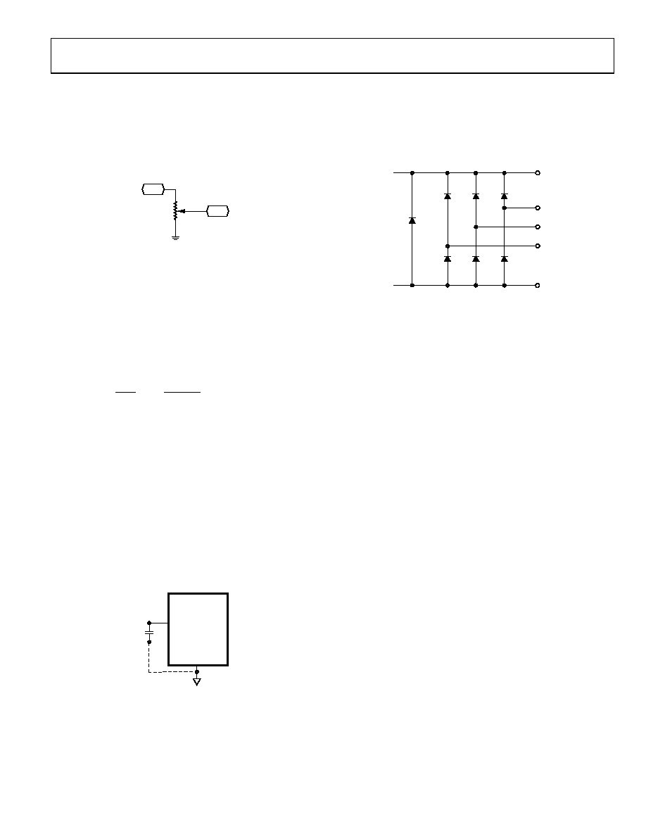
TERMINAL VOLTAGE OPERATING RANGE
The positive VDD and negative VSS power supplies of the AD5293
define the boundary conditions for proper 3-terminal, digital
potentiometer operation. Supply signals present on the A, B,
and W terminals that exceed VDD or VSS are clamped by the
internal forward-biased diodes (see Figure 50).
VSS
VDD
A
W
B
07
67
5-
04
4
Figure 50. Maximum Terminal Voltages Set by VDD and VSS
The ground pin of the AD5293 is primarily used as a digital
ground reference. To minimize the digital ground bounce, the
AD5293 ground pin should be joined remotely to common ground.
The digital input control signals to the AD5293 must be referenced
to the device ground pin (GND) to satisfy the logic level defined
in the Specifications section.
Power-Up Sequence
Because there are diodes to limit the voltage compliance at the
A, B, and W terminals (see Figure 50), it is important to power
VDD and VSS first, before applying any voltage to the A, B, and W
terminals. Otherwise, the diode is forward-biased such that VDD
and VSS are powered up unintentionally. The ideal power-up
sequence is GND, VSS, VLOGIC, VDD, the digital inputs, and then
VA, VB, and VW. The order of powering up VA, VB, VW, and the
digital inputs is not important, as long as they are powered after
VDD, VSS, and VLOGIC.
Regardless of the power-up sequence and the ramp rates of the
power supplies, the power-on preset activates after VLOGIC is
powered, restoring midscale to the RDAC register.
相关PDF资料 |
PDF描述 |
|---|---|
| VI-B40-MX-B1 | CONVERTER MOD DC/DC 5V 75W |
| VE-B2H-MY-F3 | CONVERTER MOD DC/DC 52V 50W |
| VI-BNR-IU-F1 | CONVERTER MOD DC/DC 7.5V 200W |
| VI-B3M-MX-B1 | CONVERTER MOD DC/DC 10V 75W |
| VE-B2H-MY-F2 | CONVERTER MOD DC/DC 52V 50W |
相关代理商/技术参数 |
参数描述 |
|---|---|
| AD5293BRUZ-100-RL7 | 功能描述:IC DGTL POT 1024POS 100K 14TSSOP RoHS:是 类别:集成电路 (IC) >> 数据采集 - 数字电位器 系列:- 标准包装:3,000 系列:DPP 接片:32 电阻(欧姆):10k 电路数:1 温度系数:标准值 300 ppm/°C 存储器类型:非易失 接口:3 线串行(芯片选择,递增,增/减) 电源电压:2.5 V ~ 6 V 工作温度:-40°C ~ 85°C 安装类型:表面贴装 封装/外壳:8-WFDFN 裸露焊盘 供应商设备封装:8-TDFN(2x3) 包装:带卷 (TR) |
| AD5293BRUZ-20 | 功能描述:IC DGTL POT 1024POS 20K 14TSSOP RoHS:是 类别:集成电路 (IC) >> 数据采集 - 数字电位器 系列:- 产品培训模块:Lead (SnPb) Finish for COTS Obsolescence Mitigation Program 标准包装:1 系列:- 接片:256 电阻(欧姆):100k 电路数:1 温度系数:标准值 35 ppm/°C 存储器类型:非易失 接口:3 线串口 电源电压:2.7 V ~ 5.25 V 工作温度:-40°C ~ 85°C 安装类型:表面贴装 封装/外壳:8-WDFN 裸露焊盘 供应商设备封装:8-TDFN-EP(3x3) 包装:剪切带 (CT) 产品目录页面:1399 (CN2011-ZH PDF) 其它名称:MAX5423ETA+TCT |
| AD5293BRUZ-20-RL7 | 功能描述:IC DGTL POT 1024POS 20K 14TSSOP RoHS:是 类别:集成电路 (IC) >> 数据采集 - 数字电位器 系列:- 标准包装:3,000 系列:DPP 接片:32 电阻(欧姆):10k 电路数:1 温度系数:标准值 300 ppm/°C 存储器类型:非易失 接口:3 线串行(芯片选择,递增,增/减) 电源电压:2.5 V ~ 6 V 工作温度:-40°C ~ 85°C 安装类型:表面贴装 封装/外壳:8-WFDFN 裸露焊盘 供应商设备封装:8-TDFN(2x3) 包装:带卷 (TR) |
| AD5293BRUZ-50 | 功能描述:IC DGTL POT 1024POS 50K 14TSSOP RoHS:是 类别:集成电路 (IC) >> 数据采集 - 数字电位器 系列:- 产品培训模块:Lead (SnPb) Finish for COTS Obsolescence Mitigation Program 标准包装:1 系列:- 接片:256 电阻(欧姆):100k 电路数:1 温度系数:标准值 35 ppm/°C 存储器类型:非易失 接口:3 线串口 电源电压:2.7 V ~ 5.25 V 工作温度:-40°C ~ 85°C 安装类型:表面贴装 封装/外壳:8-WDFN 裸露焊盘 供应商设备封装:8-TDFN-EP(3x3) 包装:剪切带 (CT) 产品目录页面:1399 (CN2011-ZH PDF) 其它名称:MAX5423ETA+TCT |
| AD5293BRUZ-50-RL7 | 功能描述:IC DGTL POT 1024POS 50K 14TSSOP RoHS:是 类别:集成电路 (IC) >> 数据采集 - 数字电位器 系列:- 标准包装:3,000 系列:DPP 接片:32 电阻(欧姆):10k 电路数:1 温度系数:标准值 300 ppm/°C 存储器类型:非易失 接口:3 线串行(芯片选择,递增,增/减) 电源电压:2.5 V ~ 6 V 工作温度:-40°C ~ 85°C 安装类型:表面贴装 封装/外壳:8-WFDFN 裸露焊盘 供应商设备封装:8-TDFN(2x3) 包装:带卷 (TR) |
发布紧急采购,3分钟左右您将得到回复。