- 您现在的位置:买卖IC网 > PDF目录9424 > AD5293BRUZ-20 (Analog Devices Inc)IC DGTL POT 1024POS 20K 14TSSOP PDF资料下载
参数资料
| 型号: | AD5293BRUZ-20 |
| 厂商: | Analog Devices Inc |
| 文件页数: | 15/24页 |
| 文件大小: | 0K |
| 描述: | IC DGTL POT 1024POS 20K 14TSSOP |
| 标准包装: | 96 |
| 接片: | 1024 |
| 电阻(欧姆): | 20k |
| 电路数: | 1 |
| 温度系数: | 标准值 35 ppm/°C |
| 存储器类型: | 易失 |
| 接口: | 4 线串行 |
| 电源电压: | 9 V ~ 33 V,±9 V ~ 16.5 V |
| 工作温度: | -40°C ~ 105°C |
| 安装类型: | 表面贴装 |
| 封装/外壳: | 14-TSSOP(0.173",4.40mm 宽) |
| 供应商设备封装: | 14-TSSOP |
| 包装: | 管件 |
| 产品目录页面: | 787 (CN2011-ZH PDF) |
| 其它名称: | AD5293BRUZ-20-U1 AD5293BRUZ-20-U1-ND |
AD5293
Rev. D | Page 22 of 24
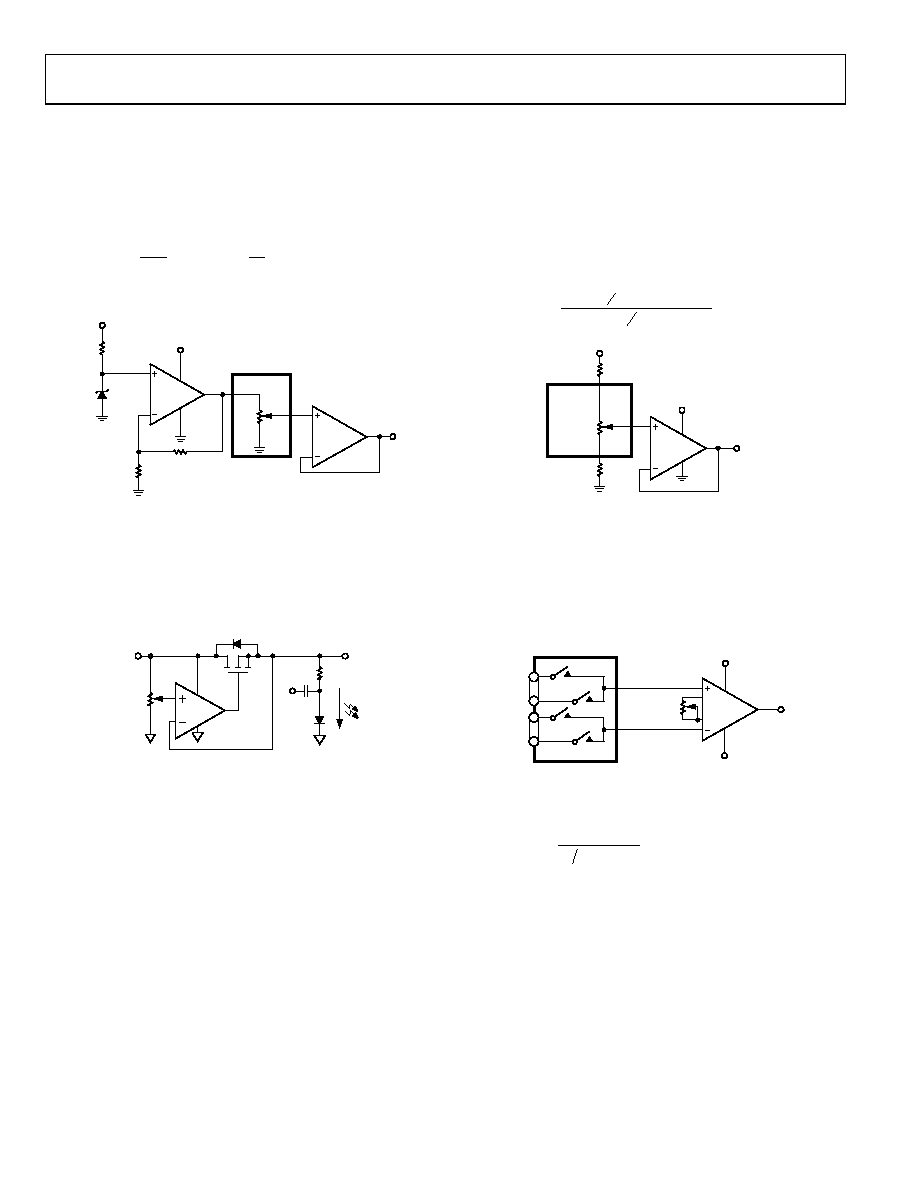
APPLICATIONS INFORMATION
HIGH VOLTAGE DAC
The AD5293 can be configured as a high voltage DAC, with an
output voltage as high as 33 V. The circuit is shown in Figure 51.
The output is
+
×
=
1
2
1
V
2
.
1
1024
)
(
R
D
V
OUT
(4)
where D is the decimal code from 0 to 1023.
AD5293
U2
AD8512
V+
V–
AD8512
VOUT
VDD
U1B
VDD
RBIAS
ADR512
D1
R2
R1
B
20k
U1A
07
675-
153
Figure 51. High Voltage DAC
PROGRAMMABLE VOLTAGE SOURCE WITH
BOOSTED OUTPUT
For applications that require high current adjustments, such as
a laser diode or turnable laser, a boosted voltage source can be
considered (see Figure 52).
W
SIGNAL
CC
RBIAS
LD
VIN
A
B
VOUT
U1
AD5293
U3 2N7002
U2
IL
OP184
07
67
5-
1
55
Figure 52. Programmable Boosted Voltage Source
In this circuit, the inverting input of the op amp forces VOUT to
be equal to the wiper voltage set by the digital potentiometer.
The load current is then delivered by the supply via the N-channel
FET (U3). The N-channel FET power handling must be adequate
to dissipate (VIN VOUT) × IL power. This circuit can source a
maximum of 100 mA with a 33 V supply.
HIGH ACCURACY DAC
It is possible to configure the AD5293 as a high accuracy DAC
by optimizing the resolution of the device over a specific reduced
voltage range. This is achieved by placing external resistors on
either side of the RDAC, as shown in Figure 53. The improved
±1% resistor tolerance specification greatly reduces error
associated with matching to discrete resistors.
3
1024
)
1024
(
1
1024
3
)
(
)
(
)
(
R
V
R
D
V
AB
D
DD
AB
D
OUT
+
×
+
×
+
=
(5)
AD5293
U1
VOUT
B
R2
20k
R1
R3
±1%
OP1177
V+
V–
VDD
U2
07
67
5-
1
54
Figure 53. Optimizing Resolution
VARIABLE GAIN INSTRUMENTATION AMPLIFIER
as shown in Figure 54, make an excellent instrumentation
amplifier for use in data acquisition systems. The data acquisition
system is low distortion and low noise enable it to condition
signals in front of a variety of ADCs.
AD8221
AD5293
+VIN1
VDD
VOUT
VSS
ADG1207
+VIN4
–VIN1
–VIN4
07
67
5-
15
6
Figure 54. Data Acquisition System
The gain can be calculated by using Equation 6, as follows:
AB
R
D
G
×
+
=
)
1024
(
kΩ
4
.
49
1
)
(
(6)
相关PDF资料 |
PDF描述 |
|---|---|
| VI-B2V-MX-B1 | CONVERTER MOD DC/DC 5.8V 75W |
| VI-BNN-IU-F4 | CONVERTER MOD DC/DC 18.5V 200W |
| VI-B2P-MX-B1 | CONVERTER MOD DC/DC 13.8V 75W |
| VE-B24-MY-F3 | CONVERTER MOD DC/DC 48V 50W |
| VI-B2J-MX-B1 | CONVERTER MOD DC/DC 36V 75W |
相关代理商/技术参数 |
参数描述 |
|---|---|
| AD5293BRUZ-20-RL7 | 功能描述:IC DGTL POT 1024POS 20K 14TSSOP RoHS:是 类别:集成电路 (IC) >> 数据采集 - 数字电位器 系列:- 标准包装:3,000 系列:DPP 接片:32 电阻(欧姆):10k 电路数:1 温度系数:标准值 300 ppm/°C 存储器类型:非易失 接口:3 线串行(芯片选择,递增,增/减) 电源电压:2.5 V ~ 6 V 工作温度:-40°C ~ 85°C 安装类型:表面贴装 封装/外壳:8-WFDFN 裸露焊盘 供应商设备封装:8-TDFN(2x3) 包装:带卷 (TR) |
| AD5293BRUZ-50 | 功能描述:IC DGTL POT 1024POS 50K 14TSSOP RoHS:是 类别:集成电路 (IC) >> 数据采集 - 数字电位器 系列:- 产品培训模块:Lead (SnPb) Finish for COTS Obsolescence Mitigation Program 标准包装:1 系列:- 接片:256 电阻(欧姆):100k 电路数:1 温度系数:标准值 35 ppm/°C 存储器类型:非易失 接口:3 线串口 电源电压:2.7 V ~ 5.25 V 工作温度:-40°C ~ 85°C 安装类型:表面贴装 封装/外壳:8-WDFN 裸露焊盘 供应商设备封装:8-TDFN-EP(3x3) 包装:剪切带 (CT) 产品目录页面:1399 (CN2011-ZH PDF) 其它名称:MAX5423ETA+TCT |
| AD5293BRUZ-50-RL7 | 功能描述:IC DGTL POT 1024POS 50K 14TSSOP RoHS:是 类别:集成电路 (IC) >> 数据采集 - 数字电位器 系列:- 标准包装:3,000 系列:DPP 接片:32 电阻(欧姆):10k 电路数:1 温度系数:标准值 300 ppm/°C 存储器类型:非易失 接口:3 线串行(芯片选择,递增,增/减) 电源电压:2.5 V ~ 6 V 工作温度:-40°C ~ 85°C 安装类型:表面贴装 封装/外壳:8-WFDFN 裸露焊盘 供应商设备封装:8-TDFN(2x3) 包装:带卷 (TR) |
| AD-52PL-711A/E | 制造商:ICE TECHNOLOGY 功能描述:IC SPECIFIC ADAPTER, 52-PLCC TO 40-DIP, Convert From:52-PLCC, Convert To:40-DIP, |
| AD52YBD | 制造商:n/a 功能描述:_ |
发布紧急采购,3分钟左右您将得到回复。