- 您现在的位置:买卖IC网 > PDF目录373875 > AD5300BRT-500RL7 (ANALOG DEVICES INC) +2.7 V to +5.5 V, 140 uA, Rail-to-Rail Output 8-Bit DAC in an SOT-23 PDF资料下载
参数资料
| 型号: | AD5300BRT-500RL7 |
| 厂商: | ANALOG DEVICES INC |
| 元件分类: | DAC |
| 英文描述: | +2.7 V to +5.5 V, 140 uA, Rail-to-Rail Output 8-Bit DAC in an SOT-23 |
| 中文描述: | SERIAL INPUT LOADING, 4 us SETTLING TIME, 8-BIT DAC, PDSO6 |
| 封装: | MO-178AB, SOT-23, 6 PIN |
| 文件页数: | 10/12页 |
| 文件大小: | 197K |
| 代理商: | AD5300BRT-500RL7 |
AD5300
–10–
REV. C
*
ADDITIONAL PINS OMITTED FOR CLARITY
SYNC
DIN
AD5300
*
SCLK
MICROWIRE
*
SK
SO
CS
Figure 28. AD5300 to MICROWIRE Interface
APPLICATIONS
Using REF19x as a Power Supply for AD5300
Because the supply current required by the AD5300 is extremely
low, an alternative option is to use a REF19x voltage reference
(REF195 for 5 V or REF193 for 3 V) to supply the required
voltage to the part—see Figure 29. This is especially useful if
your power supply is quite noisy or if the system supply voltages
are at some value other than 5 V or 3 V (e.g., 15 V). The REF19x
will output a steady supply voltage for the AD5300. If the low
dropout REF195 is used, the current it needs to supply to the
AD5300 is 140
μ
A. This is with no load on the output of the
DAC. When the DAC output is loaded, the REF195 also needs to
supply the current to the load. The total current required (with
a 5 k
load on the DAC output) is
140
μ
A + (5 V/5 k
) = 1.14 mA
The load regulation of the REF195 is typically 2 ppm/mA,
which results in an error of 2.3 ppm (11.5
μ
V) for the 1.14 mA
current drawn from it. This corresponds to a 0.0006 LSB error.
AD5300
3-WIRE
SERIAL
INTERFACE
SYNC
SCLK
DIN
15V
5V
140 A
V
OUT
= 0V TO 5V
REF195
Figure 29. REF195 as Power Supply to AD5300
Bipolar Operation Using the AD5300
The AD5300 has been designed for single-supply operation,
but a bipolar output range is also possible using the circuit in
Figure 30. The circuit in Figure 30 will give an output voltage
range of
±
5 V. Rail-to-rail operation at the amplifier output is
achievable using an AD820 or an OP295 as the output amplifier.
The output voltage for any input code can be calculated as
V
V
D
R
R
R
V
R
R
O
DD
DD
=
×
×
+
×
256
1
2
1
2
1
–
where
D
represents the input code in decimal (0 to 255).
With
V
DD
= 5 V,
R1
=
R2
= 10 k
,
V
O
=
10
×
D
256
–5
V
This is an output voltage range of
±
5 V with 00 Hex corresponding
to a –5 V output and FF Hex corresponding to a 5 V output.
AD5300 to 68HC11/68L11 Interface
Figure 26 shows a serial interface between the AD5300 and the
68HC11/68L11 microcontroller. SCK of the 68HC11/68L11
drives the SCLK of the AD5300, while the MOSI output drives
the serial data line of the DAC. The
SYNC
signal is derived
from a port line (PC7). The setup conditions for correct opera-
tion of this interface are as follows: the 68HC11/68L11 should
be configured so that its CPOL bit is a 0 and its CPHA bit is a
1. When data is being transmitted to the DAC, the
SYNC
line is
taken low (PC7). When the 68HC11/68L11 is configured as
above, data appearing on the MOSI output is valid on the falling
edge of SCK. Serial data from the 68HC11/68L11 is transmit-
ted in 8-bit bytes with only eight falling clock edges occurring in
the transmit cycle. Data is transmitted MSB first. In order to
load data to the AD5300, PC7 is left low after the first eight bits
are transferred, and a second serial write operation is performed
to the DAC and PC7 is taken high at the end of this procedure.
*
ADDITIONAL PINS OMITTED FOR CLARITY
SYNC
DIN
AD5300
*
SCLK
68HC11/68L11
*
SCK
MOSI
PC7
Figure 26. AD5300 to 68HC11/68L11 Interface
AD5300 to 80C51/80L51 Interface
Figure 27 shows a serial interface between the AD5300 and the
80C51/80L51 microcontroller. The setup for the interface is as
follows: TXD of the 80C51/80L51 drives SCLK of the AD5300,
while RXD drives the serial data line of the part. The
SYNC
signal is again derived from a bit programmable pin on the port.
In this case, port line P3.3 is used. When data is to be transmitted
to the AD5300, P3.3 is taken low. The 80C51/80L51 transmits
data only in 8-bit bytes; thus, only eight falling clock edges
occur in the transmit cycle. To load data to the DAC, P3.3 is
left low after the first eight bits are transmitted, and a second write
cycle is initiated to transmit the second byte of data. P3.3 is taken
high following the completion of this cycle. The 80C51/80L51
outputs the serial data in a format that has the LSB first. The
AD5300 requires its data with the MSB as the first bit received.
The 80C51/80L51 transmit routine takes this into account.
*
ADDITIONAL PINS OMITTED FOR CLARITY
SYNC
DIN
AD5300
*
SCLK
80C51/80L51
*
TXD
RXD
P3.3
Figure 27. AD5300 to 80C51/80L51 Interface
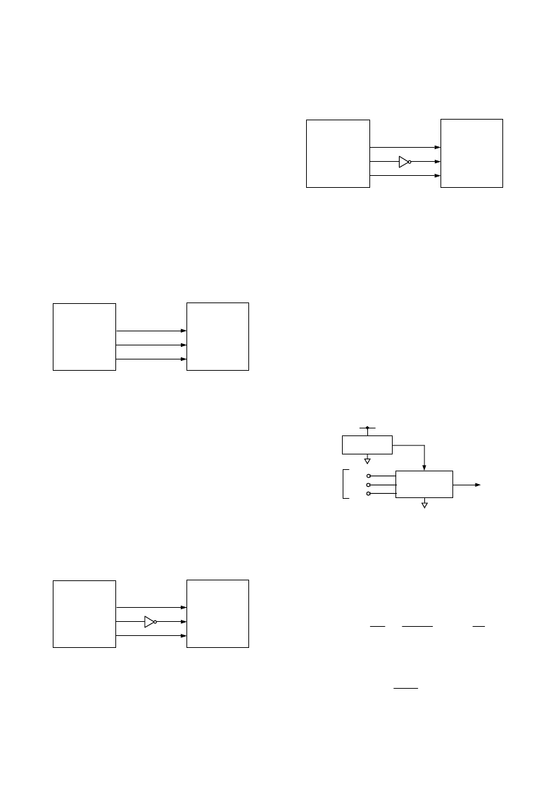
AD5300 to MICROWIRE Interface
Figure 28 shows an interface between the AD5300 and any
MICROWIRE compatible device. Serial data is shifted out on the
falling edge of the serial clock and is clocked into the AD5300 on
the rising edge of the SK.
相关PDF资料 |
PDF描述 |
|---|---|
| AD5300BRT-REEL | +2.7 V to +5.5 V, 140 uA, Rail-to-Rail Output 8-Bit DAC in an SOT-23 |
| AD5300BRT-REEL7 | +2.7 V to +5.5 V, 140 uA, Rail-to-Rail Output 8-Bit DAC in an SOT-23 |
| AD5300BRTZ-500RL7 | +2.7 V to +5.5 V, 140 uA, Rail-to-Rail Output 8-Bit DAC in an SOT-23 |
| AD5300BRTZ-REEL | +2.7 V to +5.5 V, 140 uA, Rail-to-Rail Output 8-Bit DAC in an SOT-23 |
| AD5300BRTZ-REEL7 | +2.7 V to +5.5 V, 140 uA, Rail-to-Rail Output 8-Bit DAC in an SOT-23 |
相关代理商/技术参数 |
参数描述 |
|---|---|
| AD5300BRT-R2 | 功能描述:INTEGRATED CIRCUIT 制造商:analog devices inc. 系列:* 包装:带卷(TR) 零件状态:最後搶購 封装/外壳:SOT-23-6 供应商器件封装:SOT-23-6 标准包装:1 |
| AD5300BRT-REEL | 功能描述:IC DAC 8BIT R-R 2.7-5.5V SOT23-6 RoHS:否 类别:集成电路 (IC) >> 数据采集 - 数模转换器 系列:- 标准包装:2,400 系列:- 设置时间:- 位数:18 数据接口:串行 转换器数目:3 电压电源:模拟和数字 功率耗散(最大):- 工作温度:-40°C ~ 85°C 安装类型:表面贴装 封装/外壳:36-TFBGA 供应商设备封装:36-TFBGA 包装:带卷 (TR) 输出数目和类型:* 采样率(每秒):* |
| AD5300BRT-REEL7 | 功能描述:IC DAC 8BIT R-R 2.7-5.5V SOT23-6 RoHS:否 类别:集成电路 (IC) >> 数据采集 - 数模转换器 系列:- 产品培训模块:Data Converter Fundamentals DAC Architectures 设计资源:Unipolar, Precision DC Digital-to-Analog Conversion using AD5450/1/2/3 8-14-Bit DACs (CN0052) Precision, Bipolar, Configuration for AD5450/1/2/3 8-14bit Multiplying DACs (CN0053) AC Signal Processing Using AD5450/1/2/3 Current Output DACs (CN0054) Programmable Gain Element Using AD5450/1/2/3 Current Output DAC Family (CN0055) Single Supply Low Noise LED Current Source Driver Using a Current Output DAC in the Reverse Mode (CN0139) 标准包装:10,000 系列:- 设置时间:- 位数:12 数据接口:DSP,MICROWIRE?,QSPI?,串行,SPI? 转换器数目:1 电压电源:单电源 功率耗散(最大):- 工作温度:-40°C ~ 125°C 安装类型:表面贴装 封装/外壳:SOT-23-8 薄型,TSOT-23-8 供应商设备封装:TSOT-23-8 包装:带卷 (TR) 输出数目和类型:1 电流,单极;1 电流,双极 采样率(每秒):2.7M |
| AD5300BRTZ-500RL7 | 功能描述:IC DAC 8BIT R-R 2.7-5.5V SOT23-6 RoHS:是 类别:集成电路 (IC) >> 数据采集 - 数模转换器 系列:- 产品培训模块:Data Converter Fundamentals DAC Architectures 设计资源:Unipolar, Precision DC Digital-to-Analog Conversion using AD5450/1/2/3 8-14-Bit DACs (CN0052) Precision, Bipolar, Configuration for AD5450/1/2/3 8-14bit Multiplying DACs (CN0053) AC Signal Processing Using AD5450/1/2/3 Current Output DACs (CN0054) Programmable Gain Element Using AD5450/1/2/3 Current Output DAC Family (CN0055) Single Supply Low Noise LED Current Source Driver Using a Current Output DAC in the Reverse Mode (CN0139) 标准包装:10,000 系列:- 设置时间:- 位数:12 数据接口:DSP,MICROWIRE?,QSPI?,串行,SPI? 转换器数目:1 电压电源:单电源 功率耗散(最大):- 工作温度:-40°C ~ 125°C 安装类型:表面贴装 封装/外壳:SOT-23-8 薄型,TSOT-23-8 供应商设备封装:TSOT-23-8 包装:带卷 (TR) 输出数目和类型:1 电流,单极;1 电流,双极 采样率(每秒):2.7M |
| AD5300BRTZ-REEL | 功能描述:IC DAC 8BIT R-R 2.7-5.5V SOT23-6 RoHS:是 类别:集成电路 (IC) >> 数据采集 - 数模转换器 系列:- 产品培训模块:Data Converter Fundamentals DAC Architectures 设计资源:Unipolar, Precision DC Digital-to-Analog Conversion using AD5450/1/2/3 8-14-Bit DACs (CN0052) Precision, Bipolar, Configuration for AD5450/1/2/3 8-14bit Multiplying DACs (CN0053) AC Signal Processing Using AD5450/1/2/3 Current Output DACs (CN0054) Programmable Gain Element Using AD5450/1/2/3 Current Output DAC Family (CN0055) Single Supply Low Noise LED Current Source Driver Using a Current Output DAC in the Reverse Mode (CN0139) 标准包装:10,000 系列:- 设置时间:- 位数:12 数据接口:DSP,MICROWIRE?,QSPI?,串行,SPI? 转换器数目:1 电压电源:单电源 功率耗散(最大):- 工作温度:-40°C ~ 125°C 安装类型:表面贴装 封装/外壳:SOT-23-8 薄型,TSOT-23-8 供应商设备封装:TSOT-23-8 包装:带卷 (TR) 输出数目和类型:1 电流,单极;1 电流,双极 采样率(每秒):2.7M |
发布紧急采购,3分钟左右您将得到回复。