- 您现在的位置:买卖IC网 > PDF目录373875 > AD5300BRT-REEL (ANALOG DEVICES INC) +2.7 V to +5.5 V, 140 uA, Rail-to-Rail Output 8-Bit DAC in an SOT-23 PDF资料下载
参数资料
| 型号: | AD5300BRT-REEL |
| 厂商: | ANALOG DEVICES INC |
| 元件分类: | DAC |
| 英文描述: | +2.7 V to +5.5 V, 140 uA, Rail-to-Rail Output 8-Bit DAC in an SOT-23 |
| 中文描述: | SERIAL INPUT LOADING, 4 us SETTLING TIME, 8-BIT DAC, PDSO6 |
| 封装: | MO-178AB, SOT-23, 6 PIN |
| 文件页数: | 11/12页 |
| 文件大小: | 197K |
| 代理商: | AD5300BRT-REEL |
AD5300
–11–
REV. C
0.1 F
V
DD
10k
POWER
10 F
V
DD
SYNC
SCLK
DATA
AD5300
5V
REGULATOR
V
DD
10k
V
DD
10k
V
OUT
DIN
SYNC
SCLK
GND
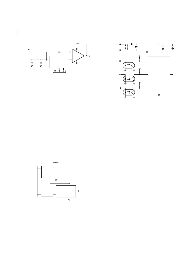
Figure 32. AD5300 with an Opto-Isolated Interface
Power Supply Bypassing and Grounding
When accuracy is important in a circuit, it is helpful to carefully
consider the power supply and ground return layout on the
board. The printed circuit board containing the AD5300 should
have separate analog and digital sections, each having its own
area of the board. If the AD5300 is in a system where other
devices require an AGND to DGND connection, the connec-
tion should be made at one point only. This ground point should
be as close as possible to the AD5300.
The power supply to the AD5300 should be bypassed with
10
μ
F and 0.1
μ
F capacitors. The capacitors should be physi-
cally as close as possible to the device with the 0.1
μ
F capacitor
ideally right up against the device. The 10
μ
F capacitors are the
tantalum bead type. It is important that the 0.1
μ
F capacitor
has low effective series resistance (ESR) and effective series
inductance (ESI), e.g., common ceramic types of capacitors. This
0.1
μ
F capacitor provides a low impedance path to ground for
high frequencies caused by transient currents due to internal
logic switching.
The power supply line itself should have as large a trace as pos-
sible to provide a low impedance path and reduce glitch effects
on the supply line. Clocks and other fast switching digital signals
should be shielded from other parts of the board by digital
ground. Avoid crossover of digital and analog signals if possible.
When traces cross on opposite sides of the board, ensure that
they run at right angles to each other to reduce feedthrough
effects through the board. The best board layout technique is
the microstrip technique where the component side of the board
is dedicated to the ground plane only and the signal traces are
placed on the solder side. However, this is not always possible
with a 2-layer board.
R2 = 10k
+5V
–5V
AD820/
OP295
3-WIRE
SERIAL
INTERFACE
+5V
AD5300
10 F
0.1 F
V
DD
V
OUT
R1 = 10k
5V
Figure 30. Bipolar Operation with the AD5300
Two 8-Bit AD5300s Together Make One 15-Bit DAC
By using the configuration in Figure 31, it can be seen that one
15-bit DAC can be made with two 8-bit AD5300s. Because of
the low supply current the AD5300 requires, the output of one
DAC may be directed into the supply pin of the second DAC.
The first DAC has no problem sourcing the required 140
μ
A
of current for the second DAC.
Since the AD5300 works on any supply voltage between 2.5 V
and 5.5 V, the output of the first DAC can be anywhere above
2.5 V. For a V
DD
of 5 V, this allows the first DAC to use half of
its output range (2.5 V to 5 V), which gives 7-bit resolution on
the output voltage. This output then becomes the supply and
reference for the second DAC. The second DAC has 8-bit reso-
lution on the output range, which gives an overall resolution for
the system of 15 bits.
A level-shifter is required to ensure that the logic input voltages
do not exceed the supply voltage of the part. The microcontroller
outputs 5 V signals, which need to be level shifted down to 2.5 V
in the case of the second DAC having a supply of only 2.5 V.
5V
MICRO-
CONTROLLER
V
OUT
= 2.5V TO 5V
LEVEL
SHIFTER
V
= 0V TO 5V
15-BIT
RESOLUTION
SYNC
SCLK
DIN
V
DD
AD5300
AD5300
V
DD
SYNC
SCLK
DIN
Figure 31. 15-Bit DAC Using Two AD5300s
Using AD5300 with an Opto-Isolated Interface
In process-control applications in industrial environments, it is
often necessary to use an opto-isolated interface to protect and
isolate the controlling circuitry from any hazardous common-
mode voltages that may occur in the area where the DAC is
functioning. Opto-isolators provide isolation in excess of 3 kV.
Because the AD5300 uses a 3-wire serial logic interface, it
requires only three opto-isolators to provide the required isola-
tion (see Figure 32). The power supply to the part also needs to
be isolated. This is done by using a transformer. On the DAC
side of the transformer, a 5 V regulator provides the 5 V supply
required for the AD5300.
相关PDF资料 |
PDF描述 |
|---|---|
| AD5300BRT-REEL7 | +2.7 V to +5.5 V, 140 uA, Rail-to-Rail Output 8-Bit DAC in an SOT-23 |
| AD5300BRTZ-500RL7 | +2.7 V to +5.5 V, 140 uA, Rail-to-Rail Output 8-Bit DAC in an SOT-23 |
| AD5300BRTZ-REEL | +2.7 V to +5.5 V, 140 uA, Rail-to-Rail Output 8-Bit DAC in an SOT-23 |
| AD5300BRTZ-REEL7 | +2.7 V to +5.5 V, 140 uA, Rail-to-Rail Output 8-Bit DAC in an SOT-23 |
| AD5300 | Rail-to-Rail Voltage Output 8-Bit DAC(满幅度电压输出8位D/A转换器) |
相关代理商/技术参数 |
参数描述 |
|---|---|
| AD5300BRT-REEL7 | 功能描述:IC DAC 8BIT R-R 2.7-5.5V SOT23-6 RoHS:否 类别:集成电路 (IC) >> 数据采集 - 数模转换器 系列:- 产品培训模块:Data Converter Fundamentals DAC Architectures 设计资源:Unipolar, Precision DC Digital-to-Analog Conversion using AD5450/1/2/3 8-14-Bit DACs (CN0052) Precision, Bipolar, Configuration for AD5450/1/2/3 8-14bit Multiplying DACs (CN0053) AC Signal Processing Using AD5450/1/2/3 Current Output DACs (CN0054) Programmable Gain Element Using AD5450/1/2/3 Current Output DAC Family (CN0055) Single Supply Low Noise LED Current Source Driver Using a Current Output DAC in the Reverse Mode (CN0139) 标准包装:10,000 系列:- 设置时间:- 位数:12 数据接口:DSP,MICROWIRE?,QSPI?,串行,SPI? 转换器数目:1 电压电源:单电源 功率耗散(最大):- 工作温度:-40°C ~ 125°C 安装类型:表面贴装 封装/外壳:SOT-23-8 薄型,TSOT-23-8 供应商设备封装:TSOT-23-8 包装:带卷 (TR) 输出数目和类型:1 电流,单极;1 电流,双极 采样率(每秒):2.7M |
| AD5300BRTZ-500RL7 | 功能描述:IC DAC 8BIT R-R 2.7-5.5V SOT23-6 RoHS:是 类别:集成电路 (IC) >> 数据采集 - 数模转换器 系列:- 产品培训模块:Data Converter Fundamentals DAC Architectures 设计资源:Unipolar, Precision DC Digital-to-Analog Conversion using AD5450/1/2/3 8-14-Bit DACs (CN0052) Precision, Bipolar, Configuration for AD5450/1/2/3 8-14bit Multiplying DACs (CN0053) AC Signal Processing Using AD5450/1/2/3 Current Output DACs (CN0054) Programmable Gain Element Using AD5450/1/2/3 Current Output DAC Family (CN0055) Single Supply Low Noise LED Current Source Driver Using a Current Output DAC in the Reverse Mode (CN0139) 标准包装:10,000 系列:- 设置时间:- 位数:12 数据接口:DSP,MICROWIRE?,QSPI?,串行,SPI? 转换器数目:1 电压电源:单电源 功率耗散(最大):- 工作温度:-40°C ~ 125°C 安装类型:表面贴装 封装/外壳:SOT-23-8 薄型,TSOT-23-8 供应商设备封装:TSOT-23-8 包装:带卷 (TR) 输出数目和类型:1 电流,单极;1 电流,双极 采样率(每秒):2.7M |
| AD5300BRTZ-REEL | 功能描述:IC DAC 8BIT R-R 2.7-5.5V SOT23-6 RoHS:是 类别:集成电路 (IC) >> 数据采集 - 数模转换器 系列:- 产品培训模块:Data Converter Fundamentals DAC Architectures 设计资源:Unipolar, Precision DC Digital-to-Analog Conversion using AD5450/1/2/3 8-14-Bit DACs (CN0052) Precision, Bipolar, Configuration for AD5450/1/2/3 8-14bit Multiplying DACs (CN0053) AC Signal Processing Using AD5450/1/2/3 Current Output DACs (CN0054) Programmable Gain Element Using AD5450/1/2/3 Current Output DAC Family (CN0055) Single Supply Low Noise LED Current Source Driver Using a Current Output DAC in the Reverse Mode (CN0139) 标准包装:10,000 系列:- 设置时间:- 位数:12 数据接口:DSP,MICROWIRE?,QSPI?,串行,SPI? 转换器数目:1 电压电源:单电源 功率耗散(最大):- 工作温度:-40°C ~ 125°C 安装类型:表面贴装 封装/外壳:SOT-23-8 薄型,TSOT-23-8 供应商设备封装:TSOT-23-8 包装:带卷 (TR) 输出数目和类型:1 电流,单极;1 电流,双极 采样率(每秒):2.7M |
| AD5300BRTZ-REEL7 | 功能描述:IC DAC 8BIT R-R 2.7-5.5V SOT23-6 RoHS:是 类别:集成电路 (IC) >> 数据采集 - 数模转换器 系列:- 产品培训模块:Data Converter Fundamentals DAC Architectures 标准包装:3,000 系列:nanoDAC™ 设置时间:80µs 位数:18 数据接口:DSP,MICROWIRE?,QSPI?,串行,SPI? 转换器数目:1 电压电源:单电源 功率耗散(最大):- 工作温度:-40°C ~ 105°C 安装类型:表面贴装 封装/外壳:SOT-23-8 供应商设备封装:SOT-23-8 包装:带卷 (TR) 输出数目和类型:1 电压,单极 采样率(每秒):- 产品目录页面:784 (CN2011-ZH PDF) 配用:EVAL-AD5680EBZ-ND - BOARD EVAL FOR AD5680 其它名称:AD5680BRJZ-2REEL7TR |
| AD5300OKHJBOX | 制造商:Advanced Micro Devices 功能描述:AMD A-SERIES APU A4-5300 X2 3400MHZ 1MB FM2 65W PIB - Boxed Product (Development Kits) |
发布紧急采购,3分钟左右您将得到回复。