- 您现在的位置:买卖IC网 > PDF目录10791 > AD5302BRMZ-REEL (Analog Devices Inc)IC DAC 8BIT DUAL R-R 10-MSOP PDF资料下载
参数资料
| 型号: | AD5302BRMZ-REEL |
| 厂商: | Analog Devices Inc |
| 文件页数: | 23/24页 |
| 文件大小: | 0K |
| 描述: | IC DAC 8BIT DUAL R-R 10-MSOP |
| 产品培训模块: | Data Converter Fundamentals DAC Architectures |
| 产品变化通告: | Product Discontinuance 27/Oct/2011 |
| 标准包装: | 3,000 |
| 设置时间: | 6µs |
| 位数: | 8 |
| 数据接口: | 串行 |
| 转换器数目: | 2 |
| 电压电源: | 单电源 |
| 功率耗散(最大): | 2.5mW |
| 工作温度: | -40°C ~ 105°C |
| 安装类型: | 表面贴装 |
| 封装/外壳: | 10-TFSOP,10-MSOP(0.118",3.00mm 宽) |
| 供应商设备封装: | 10-MSOP |
| 包装: | 带卷 (TR) |
| 输出数目和类型: | 2 电压,单极;2 电压,双极 |
| 采样率(每秒): | 167k |
AD5302/AD5312/AD5322
Rev. D | Page 8 of 24
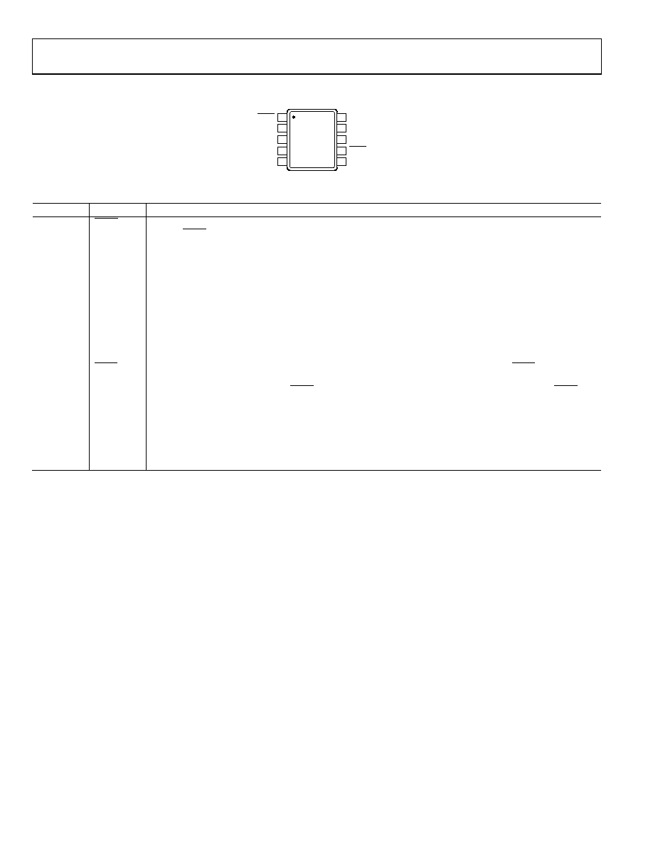
PIN CONFIGURATION AND FUNCTION DESCRIPTIONS
LDAC 1
VDD 2
VREFB 3
VREFA 4
VOUTA 5
GND
10
DIN
9
SCLK
8
SYNC
7
VOUTB
6
AD5302/
AD5312/
AD5322
TOP VIEW
(Not to Scale)
00
92
8-
00
3
Figure 5. Pin Configuration
Table 5. Pin Function Descriptions
Pin No.
Mnemonic
Description
1
LDAC
Active Low Control Input. This pin transfers the contents of the input registers to their respective DAC registers.
Pulsing LDAC low allows either or both DAC registers to be updated if the input registers have new data. This
allows simultaneous updating of both DAC outputs.
2
VDD
Power Supply Input. The parts can be operated from 2.5 V to 5.5 V, and the supply should be decoupled to GND.
3
VREFB
Reference Input Pin for DAC B. This is the reference for DAC B. It can be configured as a buffered or an
unbuffered input, depending on the BUF bit in the control word of DAC B. It has an input range of 0 V to VDD in
unbuffered mode and 1 V to VDD in buffered mode.
4
VREFA
Reference Input Pin for DAC A. This is the reference for DAC A. It can be configured as a buffered or an
unbuffered input depending on the BUF bit in the control word of DAC A. It has an input range of 0 V to VDD in
unbuffered mode and 1 V to VDD in buffered mode.
5
VOUTA
Buffered Analog Output Voltage from DAC A. The output amplifier has rail-to-rail operation.
6
VOUTB
Buffered Analog Output Voltage from DAC B. The output amplifier has rail-to-rail operation.
7
SYNC
Active Low Control Input. This is the frame synchronization signal for the input data. When SYNC goes low, it
powers on the SCLK and DIN buffers and enables the input shift register. Data is transferred in on the falling
edges of the following 16 clocks. If SYNC is taken high before the 16th falling edge, the rising edge of SYNC acts
as an interrupt and the write sequence is ignored by the device.
8
SCLK
Serial Clock Input. Data is clocked into the input shift register on the falling edge of the serial clock input. Data
can be transferred at rates up to 30 MHz. The SCLK input buffer is powered down after each write cycle.
9
DIN
Serial Data Input. This device has a 16-bit input shift register. Data is clocked into the register on the falling
edge of the serial clock input. The DIN input buffer is powered down after each write cycle.
10
GND
Ground Reference Point for All Circuitry on the Part.
相关PDF资料 |
PDF描述 |
|---|---|
| VI-24B-CU-F4 | CONVERTER MOD DC/DC 95V 200W |
| AD8612ARUZ | IC COMP DUAL 4NS FAST 14-TSSOP |
| VI-244-IW-S | CONVERTER MOD DC/DC 48V 100W |
| AD5301BRTZ-REEL | IC DAC 8BIT 2WIRE I2C SOT23-6 |
| B37981M1682K054 | CAP CER 6800PF 100V 10% RADIAL |
相关代理商/技术参数 |
参数描述 |
|---|---|
| AD5302BRMZ-REEL7 | 功能描述:IC DAC 8BIT DUAL R-R 10-MSOP RoHS:是 类别:集成电路 (IC) >> 数据采集 - 数模转换器 系列:- 标准包装:1 系列:- 设置时间:4.5µs 位数:12 数据接口:串行,SPI? 转换器数目:1 电压电源:单电源 功率耗散(最大):- 工作温度:-40°C ~ 125°C 安装类型:表面贴装 封装/外壳:8-SOIC(0.154",3.90mm 宽) 供应商设备封装:8-SOICN 包装:剪切带 (CT) 输出数目和类型:1 电压,单极;1 电压,双极 采样率(每秒):* 其它名称:MCP4921T-E/SNCTMCP4921T-E/SNRCTMCP4921T-E/SNRCT-ND |
| AD5303 | 制造商:AD 制造商全称:Analog Devices 功能描述:2.5 V to 5.5 V, 500 uA, Parallel Interface Quad Voltage-Output 8-/10-/12-Bit DACs |
| AD53032 | 制造商:AD 制造商全称:Analog Devices 功能描述:High Performance Driver/Comparator Active Load on a Single Chip |
| AD53032JSTP | 制造商:Analog Devices 功能描述:High Performance Driver/Comparator 52-Pin LQFP |
| AD53033 | 制造商:AD 制造商全称:Analog Devices 功能描述:High Performance Driver/Comparator on a Single Chip |
发布紧急采购,3分钟左右您将得到回复。