- 您现在的位置:买卖IC网 > PDF目录10786 > AD5307BRUZ-REEL7 (Analog Devices Inc)IC DAC 8BIT QUAD W/BUFF 16TSSOP PDF资料下载
参数资料
| 型号: | AD5307BRUZ-REEL7 |
| 厂商: | Analog Devices Inc |
| 文件页数: | 22/28页 |
| 文件大小: | 0K |
| 描述: | IC DAC 8BIT QUAD W/BUFF 16TSSOP |
| 产品培训模块: | Data Converter Fundamentals DAC Architectures |
| 产品变化通告: | Product Discontinuance 27/Oct/2011 |
| 标准包装: | 1,000 |
| 设置时间: | 6µs |
| 位数: | 8 |
| 数据接口: | DSP,MICROWIRE?,QSPI?,串行,SPI? |
| 转换器数目: | 4 |
| 电压电源: | 单电源 |
| 功率耗散(最大): | 4.5mW |
| 工作温度: | -40°C ~ 105°C |
| 安装类型: | 表面贴装 |
| 封装/外壳: | 16-TSSOP(0.173",4.40mm 宽) |
| 供应商设备封装: | 16-TSSOP |
| 包装: | 带卷 (TR) |
| 输出数目和类型: | 4 电压,单极;4 电压,双极 |
| 采样率(每秒): | 167k |
第1页第2页第3页第4页第5页第6页第7页第8页第9页第10页第11页第12页第13页第14页第15页第16页第17页第18页第19页第20页第21页当前第22页第23页第24页第25页第26页第27页第28页
AD5307/AD5317/AD5327
Rev. C | Page 3 of 28
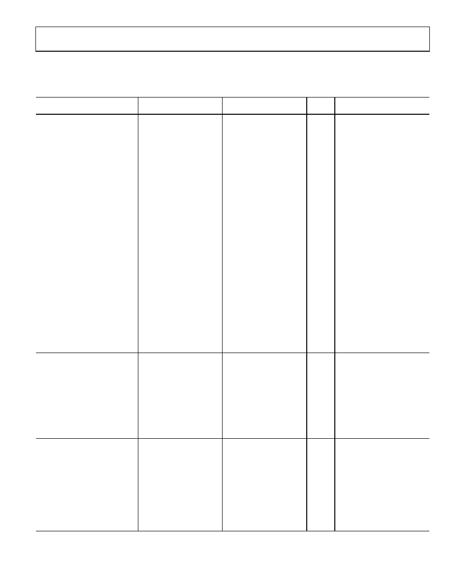
SPECIFICATIONS
VDD = 2.5 V to 5.5 V, VREF = 2 V, RL = 2 kΩ to GND, CL = 200 pF to GND. All specifications TMIN to TMAX, unless otherwise noted.
Table 1.
A Version1
B Version
Parameter2
Min
Typ
Max
Min
Typ
Max
Unit
Conditions/Comments
AD5307
Resolution
8
Bits
Relative Accuracy
±0.15
±1
±0.15
±0.625
LSB
Differential Nonlinearity
±0.02
±0.25
±0.02
±0.25
LSB
Guaranteed monotonic by design
over all codes
AD5317
Resolution
10
Bits
Relative Accuracy
±0.5
±4
±0.5
±2.5
LSB
Differential Nonlinearity
±0.05
±0.5
±0.05
±0.5
LSB
Guaranteed monotonic by design
over all codes
AD5327
Resolution
12
Bits
Relative Accuracy
±2
±16
±2
±10
LSB
Differential Nonlinearity
±0.2
±1
±0.2
±1
LSB
Guaranteed monotonic by design
over all codes
Offset Error
±5
±60
±5
±60
mV
and Figure 30
Gain Error
±0.3
±1.25
±0.3
±1.25
% FSR
and Figure 30
Lower Dead Band5
10
60
10
60
mV
See Figure 29, lower dead band
exists only if offset error is negative
Upper Dead Band
10
60
10
60
mV
See Figure 30, upper dead band
exists only if VREF = VDD and offset
plus gain error is positive
Offset Error Drift6
12
ppm of
FSR/°C
Gain Error Drift
5
ppm of
FSR/°C
DC Power Supply Rejection Ratio
60
dB
VDD = ±10%
DC Crosstalk
200
mV
RL = 2 kΩ to GND or VDD
DAC REFERENCE INPUTS
VREF Input Range
1
VDD
1
VDD
V
Buffered reference mode
0.25
VDD
0.25
VDD
V
Unbuffered reference mode
VREF Input Impedance (RDAC)
>10
MΩ
Buffered reference mode and
power-down mode
74
90
74
90
kΩ
Unbuffered reference mode,
0 V to VREF output range
37
45
37
45
kΩ
Unbuffered reference mode,
0 V to 2 VREF output range
Reference Feedthrough
90
dB
Frequency = 10 kHz
Channel-to-Channel Isolation
75
dB
Frequency = 10 kHz
OUTPUT CHARACTERISTICS
Minimum Output Voltage7
0.001
V
A measure of the minimum drive
capability of the output amplifier
Maximum Output Voltage
VDD
0.001
VDD
0.001
V
A measure of the maximum drive
capability of the output amplifier
DC Output Impedance
0.5
Ω
Short-Circuit Current
25
mA
VDD = 5 V
16
mA
VDD = 3 V
Power-Up Time
2.5
μs
Coming out of power-down mode,
VDD = 5 V
5
μs
Coming out of power-down mode,
VDD = 3 V
相关PDF资料 |
PDF描述 |
|---|---|
| VI-BNX-MX-F4 | CONVERTER MOD DC/DC 5.2V 75W |
| VI-BNX-MX-F2 | CONVERTER MOD DC/DC 5.2V 75W |
| VI-BNX-MX-F1 | CONVERTER MOD DC/DC 5.2V 75W |
| VE-J0V-MY-S | CONVERTER MOD DC/DC 5.8V 50W |
| VI-BNX-MW | CONVERTER MOD DC/DC 5.2V 100W |
相关代理商/技术参数 |
参数描述 |
|---|---|
| AD5308 | 制造商:AD 制造商全称:Analog Devices 功能描述:2.5 V to 5.5 V Octal Voltage Output 8-/10-/12-Bit DACs in 16-Lead TSSOP |
| AD5308_1 | 制造商:AD 制造商全称:Analog Devices 功能描述:2.5 V to 5.5 V Octal Voltage Output 8-/10-/12-Bit DACs in 16-Lead TSSOP |
| AD5308_11 | 制造商:AD 制造商全称:Analog Devices 功能描述:2.5 V to 5.5 V Octal Voltage Output 8-/10-/12-Bit DACs in 16-Lead TSSOP |
| AD5308ARU | 功能描述:IC DAC 8BIT OCTAL W/BUFF 16TSSOP RoHS:否 类别:集成电路 (IC) >> 数据采集 - 数模转换器 系列:- 产品培训模块:LTC263x 12-, 10-, and 8-Bit VOUT DAC Family 特色产品:LTC2636 - Octal 12-/10-/8-Bit SPI VOUT DACs with 10ppm/°C Reference 标准包装:91 系列:- 设置时间:4µs 位数:10 数据接口:MICROWIRE?,串行,SPI? 转换器数目:8 电压电源:单电源 功率耗散(最大):2.7mW 工作温度:-40°C ~ 85°C 安装类型:表面贴装 封装/外壳:14-WFDFN 裸露焊盘 供应商设备封装:14-DFN-EP(4x3) 包装:管件 输出数目和类型:8 电压,单极 采样率(每秒):* |
| AD5308ARU-REEL7 | 功能描述:IC DAC 8BIT OCTAL W/BUFF 16TSSOP RoHS:否 类别:集成电路 (IC) >> 数据采集 - 数模转换器 系列:- 产品培训模块:LTC263x 12-, 10-, and 8-Bit VOUT DAC Family 特色产品:LTC2636 - Octal 12-/10-/8-Bit SPI VOUT DACs with 10ppm/°C Reference 标准包装:91 系列:- 设置时间:4µs 位数:10 数据接口:MICROWIRE?,串行,SPI? 转换器数目:8 电压电源:单电源 功率耗散(最大):2.7mW 工作温度:-40°C ~ 85°C 安装类型:表面贴装 封装/外壳:14-WFDFN 裸露焊盘 供应商设备封装:14-DFN-EP(4x3) 包装:管件 输出数目和类型:8 电压,单极 采样率(每秒):* |
发布紧急采购,3分钟左右您将得到回复。