- 您现在的位置:买卖IC网 > PDF目录8708 > AD5307BRUZ-REEL (Analog Devices Inc)IC DAC 8BIT QUAD W/BUFF 16TSSOP PDF资料下载
参数资料
| 型号: | AD5307BRUZ-REEL |
| 厂商: | Analog Devices Inc |
| 文件页数: | 24/28页 |
| 文件大小: | 0K |
| 描述: | IC DAC 8BIT QUAD W/BUFF 16TSSOP |
| 产品培训模块: | Data Converter Fundamentals DAC Architectures |
| 产品变化通告: | Product Discontinuance 27/Oct/2011 |
| 标准包装: | 2,500 |
| 设置时间: | 6µs |
| 位数: | 8 |
| 数据接口: | DSP,MICROWIRE?,QSPI?,串行,SPI? |
| 转换器数目: | 4 |
| 电压电源: | 单电源 |
| 功率耗散(最大): | 4.5mW |
| 工作温度: | -40°C ~ 105°C |
| 安装类型: | 表面贴装 |
| 封装/外壳: | 16-TSSOP(0.173",4.40mm 宽) |
| 供应商设备封装: | 16-TSSOP |
| 包装: | 带卷 (TR) |
| 输出数目和类型: | 4 电压,单极;4 电压,双极 |
| 采样率(每秒): | 167k |
第1页第2页第3页第4页第5页第6页第7页第8页第9页第10页第11页第12页第13页第14页第15页第16页第17页第18页第19页第20页第21页第22页第23页当前第24页第25页第26页第27页第28页
AD5307/AD5317/AD5327
Rev. C | Page 5 of 28
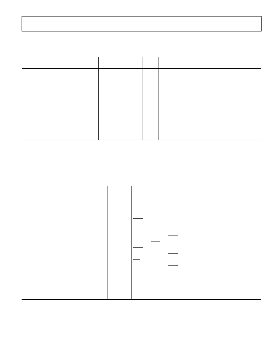
AC CHARACTERISTICS
VDD = 2.5 V to 5.5 V, RL = 2 kΩ to GND, CL = 200 pF to GND. All specifications TMIN to TMAX, unless otherwise noted.
Table 2.
A, B Versions1
Min
Typ
Max
Unit
Conditions/Comments
Output Voltage Settling Time
VREF = VDD = 5 V
AD5307
6
8
μs
1/4 scale to 3/4 scale change (0x40 to 0xC0)
AD5317
7
9
μs
1/4 scale to 3/4 scale change (0x100 to 0x300)
AD5327
8
10
μs
1/4 scale to 3/4 scale change (0x400 to 0xC00)
Slew Rate
0.7
V/μs
Major-Code Change Glitch Energy
12
nV-s
1 LSB change around major carry
Digital Feedthrough
0.5
nV-s
SDO Feedthrough
4
nV-s
Daisy-chain mode; SDO load is 10 pF
Digital Crosstalk
0.5
nV-s
Analog Crosstalk
1
nV-s
DAC-to-DAC Crosstalk
3
nV-s
Multiplying Bandwidth
200
kHz
VREF = 2 V ± 0.1 V p-p; unbuffered mode
Total Harmonic Distortion
70
dB
VREF = 2.5 V ± 0.1 V p-p; frequency = 10 kHz
1 Temperature range (A, B versions): 40°C to +105°C; typical at +25°C.
2 Guaranteed by design and characterization; not production tested.
3 See the Terminology section.
TIMING CHARACTERISTICS
VDD = 2.5 V to 5.5 V; all specifications TMIN to TMAX, unless otherwise noted.
Table 3.
A, B Versions
Parameter1, ,
Limit at TMIN, TMAX
Unit
Conditions/Comments
t1
33
ns min
SCLK cycle time
t2
13
ns min
SCLK high time
t3
13
ns min
SCLK low time
t4
13
ns min
SYNC to SCLK falling edge set-up time
t5
5
ns min
Data set-up time
t6
4.5
ns min
Data hold time
t7
5
ns min
SCLK falling edge to SYNC rising edge
t8
50
ns min
Minimum SYNC high time
t9
20
ns min
LDAC pulse width
t10
20
ns min
SCLK falling edge to LDAC rising edge
t11
20
ns min
CLR pulse width
t12
0
ns min
SCLK falling edge to LDAC falling edge
20
ns max
SCLK rising edge to SDO valid (VDD = 3.6 V to 5.5 V)
25
ns max
SCLK rising edge to SDO valid (VDD = 2.5 V to 3.5 V)
t14
5
ns min
SCLK falling edge to SYNC rising edge
t15
8
ns min
SYNC rising edge to SCLK rising edge
t16
0
ns min
SYNC rising edge to LDAC falling edge
1 Guaranteed by design and characterization; not production tested.
2 All input signals are specified with tR = tF = 5 ns (10% to 90% of VDD) and timed from a voltage level of (VIL + VIH)/2.
3 See Figure 3 and Figure 4.
4 This is measured with the load circuit of Figure 2. t13 determines maximum SCLK frequency in daisy-chain mode.
5 Daisy-chain mode only.
相关PDF资料 |
PDF描述 |
|---|---|
| V110A28H400BF3 | CONVERTER MOD DC/DC 28V 400W |
| IDT74FCT20807PYGI | IC CLK BUFF 1:10 166MHZ 20-SSOP |
| AD5306BRUZ-REEL | IC DAC 8BIT QUAD W/BUFF 16-TSSOP |
| IDT74FCT807BTSOGI8 | IC CLK BUFFER 1:10 100MHZ 20SOIC |
| VE-B6V-MV-F1 | CONVERTER MOD DC/DC 5.8V 150W |
相关代理商/技术参数 |
参数描述 |
|---|---|
| AD5307BRUZ-REEL7 | 功能描述:IC DAC 8BIT QUAD W/BUFF 16TSSOP RoHS:是 类别:集成电路 (IC) >> 数据采集 - 数模转换器 系列:- 标准包装:2,400 系列:- 设置时间:- 位数:18 数据接口:串行 转换器数目:3 电压电源:模拟和数字 功率耗散(最大):- 工作温度:-40°C ~ 85°C 安装类型:表面贴装 封装/外壳:36-TFBGA 供应商设备封装:36-TFBGA 包装:带卷 (TR) 输出数目和类型:* 采样率(每秒):* |
| AD5308 | 制造商:AD 制造商全称:Analog Devices 功能描述:2.5 V to 5.5 V Octal Voltage Output 8-/10-/12-Bit DACs in 16-Lead TSSOP |
| AD5308_1 | 制造商:AD 制造商全称:Analog Devices 功能描述:2.5 V to 5.5 V Octal Voltage Output 8-/10-/12-Bit DACs in 16-Lead TSSOP |
| AD5308_11 | 制造商:AD 制造商全称:Analog Devices 功能描述:2.5 V to 5.5 V Octal Voltage Output 8-/10-/12-Bit DACs in 16-Lead TSSOP |
| AD5308ARU | 功能描述:IC DAC 8BIT OCTAL W/BUFF 16TSSOP RoHS:否 类别:集成电路 (IC) >> 数据采集 - 数模转换器 系列:- 产品培训模块:LTC263x 12-, 10-, and 8-Bit VOUT DAC Family 特色产品:LTC2636 - Octal 12-/10-/8-Bit SPI VOUT DACs with 10ppm/°C Reference 标准包装:91 系列:- 设置时间:4µs 位数:10 数据接口:MICROWIRE?,串行,SPI? 转换器数目:8 电压电源:单电源 功率耗散(最大):2.7mW 工作温度:-40°C ~ 85°C 安装类型:表面贴装 封装/外壳:14-WFDFN 裸露焊盘 供应商设备封装:14-DFN-EP(4x3) 包装:管件 输出数目和类型:8 电压,单极 采样率(每秒):* |
发布紧急采购,3分钟左右您将得到回复。