- 您现在的位置:买卖IC网 > PDF目录373876 > AD5308 (Analog Devices, Inc.) 2.5 V to 5.5 V Octal Voltage Output 8-/10-/12-Bit DACs in 16-Lead TSSOP PDF资料下载
参数资料
| 型号: | AD5308 |
| 厂商: | Analog Devices, Inc. |
| 英文描述: | 2.5 V to 5.5 V Octal Voltage Output 8-/10-/12-Bit DACs in 16-Lead TSSOP |
| 中文描述: | 2.5 V至5.5 V电压输出8-/10-/12-Bit八路数模转换器的16引脚TSSOP |
| 文件页数: | 14/19页 |
| 文件大小: | 308K |
| 代理商: | AD5308 |
REV. B
–14–
AD5308/AD5318/AD5328
If the user wishes to update the DAC through software, the
LDAC
pin should be tied high and the
LDAC
mode bits set as required.
Alternatively, if the user wishes to control the DAC through
hardware, i.e., the
LDAC
pin, the
LDAC
mode bits should be
set to
LDAC
high (default mode).
Use of the
LDAC
function enables double-buffering of the DAC
data, and the GAIN, BUF and V
DD
bits. There are two ways in
which the
LDAC
function can operate:
Synchronous
LDAC
:
The DAC registers are updated after
new data is read in on the falling edge of the 16th SCLK pulse.
LDAC
can be permanently low or pulsed as in Figure 1.
Asynchronous
LDAC
:
The outputs are not updated at the
same time that the input registers are written to. When
LDAC
goes low, the DAC registers are updated with the contents of
the input register.
DOUBLE-BUFFERED INTERFACE
The AD5308/AD5318/AD5328 DACs all have double-buffered
interfaces consisting of two banks of registers: input and DAC.
The input registers are connected directly to the input shift
register, and the digital code is transferred to the relevant input
register on completion of a valid write sequence. The DAC
registers contain the digital code used by the resistor strings.
When the
LDAC
pin is high and the
LDAC
bits are set to (01),
the DAC registers are latched and the input registers may change
state without affecting the contents of the DAC registers. How-
ever, when the
LDAC
bits are set to (00) or when the
LDAC
pin is brought low, the DAC registers become transparent and
the contents of the input registers are transferred to them.
The double-buffered interface is useful if the user requires simulta-
neous updating of all DAC outputs. The user may write to seven
of the input registers individually and then, by bringing
LDAC
low when writing to the remaining DAC input register, all out-
puts will update simultaneously.
These parts contain an extra feature whereby a DAC register is
not updated unless its input register has been updated since the
last time
LDAC
was low. Normally, when
LDAC
is brought
low, the DAC registers are filled with the contents of the input
registers. In the case of the AD5308/AD5318/AD5328, the part
will update the DAC register only if the input register has been
changed since the last time the DAC register was updated, thereby
removing unnecessary digital crosstalk.
POWER-DOWN MODE
The AD5308/AD5318/AD5328 have low power consumption,
typically dissipating 2.4 mW with a 3 V supply and 5 mW with a
5 V supply. Power consumption can be further reduced when the
DACs are not in use by putting them into power-down mode,
which was described previously.
When in default mode, all DACs work normally with a typical
power consumption of 1 mA at 5 V (800
μ
A at 3 V). However,
when all DACs are powered down, i.e., in power-down mode,
the supply current falls to 400 nA at 5 V (120 nA at 3 V). Not
only does the supply current drop, but the output stage is also
internally switched from the output of the amplifier, making it
open-circuit. This has the advantage that the output is three-
state while the part is in power-down mode, and provides a defined
input condition for whatever is connected to the output of the
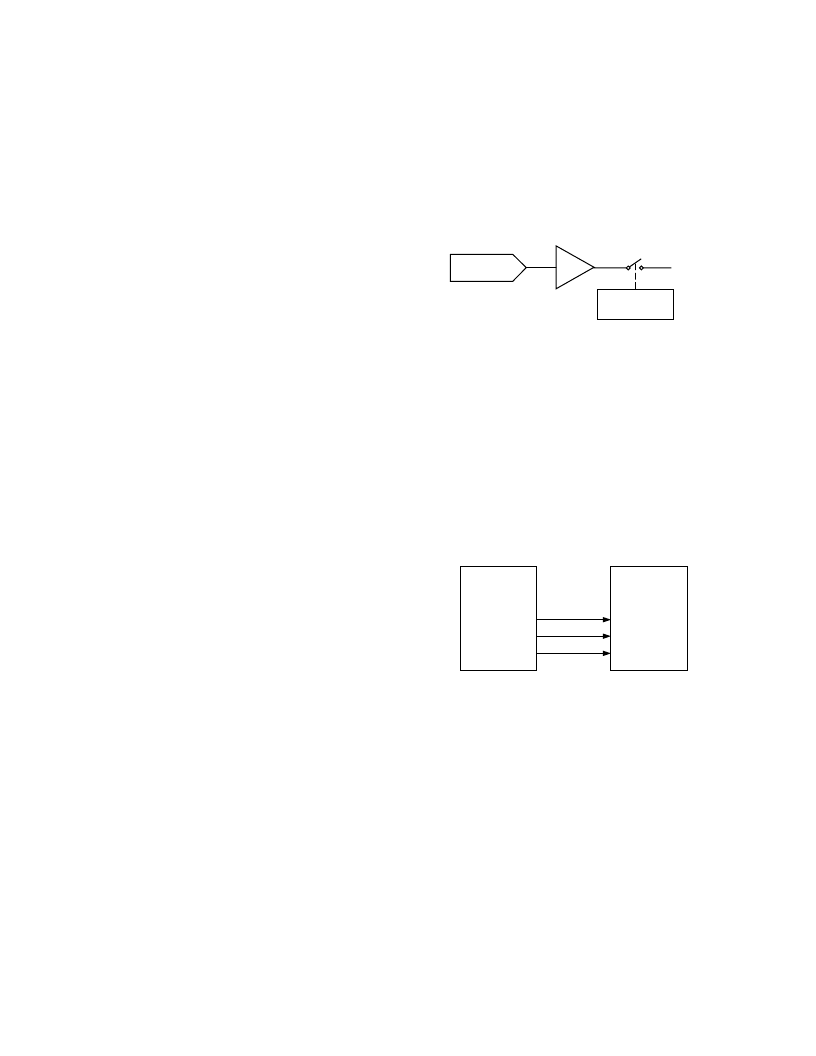
DAC amplifier. The output stage is illustrated in Figure 10.
The bias generator, the output amplifiers, the resistor string,
and all other associated linear circuitry are shut down when the
power-down mode is activated. However, the contents of the
registers are unaffected when in power-down. In fact, it is pos-
sible to load new data to the input registers and DAC registers
during power-down. The DAC outputs will update as soon as
the device comes out of power-down mode. The time to exit
power-down is typically 2.5
μ
s for V
DD
= 5 V and 5
μ
s when
V
DD
= 3 V.
RESISTOR-
STRING DAC
POWER-DOWN
CIRCUITRY
AMPLIFIER
V
OUT
Figure 10. Output Stage during Power-Down
MICROPROCESSOR INTERFACING
ADSP-2101/ADSP-2103 to AD5308/AD5318/AD5328 Interface
Figure 11 shows a serial interface between the AD5308/AD5318/
AD5328 and the ADSP-2101/ADSP-2103. The ADSP-2101/
ADSP-2103 should be set up to operate in the SPORT transmit
alternate framing mode. The ADSP-2101/ADSP-2103 SPORT
is programmed through the SPORT control register and should
be configured as follows: internal clock operation, active-low
framing, and 16-bit word length. Transmission is initiated by
writing a word to the Tx register after the SPORT has been
enabled. The data is clocked out on each rising edge of the
DSP’s serial clock and clocked into the AD5308/AD5318/
AD5328 on the falling edge of the DAC’s SCLK.
AD5308/
AD5318/
AD5328
*
SCLK
DIN
SYNC
TFS
DT
SCLK
ADSP-2101/
ADSP-2103
*
*
ADDITIONAL PINS OMITTED FOR CLARITY
Figure 11. ADSP-2101/ADSP-2103 to AD5308
AD5318/AD5328 Interface
68HC11/68L11 to AD5308/AD5318/AD5328 Interface
Figure 12 shows a serial interface between the AD5308/AD5318/
AD5328 and the 68HC11/68L11 microcontroller. SCK of the
68HC11/68L11 drives the SCLK of the AD5308/AD5318/
AD5328, while the MOSI output drives the serial data line
(DIN) of the DAC. The
SYNC
signal is derived from a port
line (PC7). The setup conditions for the correct operation of
this interface are as follows: the 68HC11/68L11 should be
configured so that its CPOL bit is a 0 and its CPHA bit is a 1.
When data is being transmitted to the DAC, the
SYNC
line is
taken low (PC7). When the 68HC11/68L11 is configured as
above, data appearing on the MOSI output is valid on the falling
edge of SCK. Serial data from the 68HC11/68L11 is transmit-
ted in 8-bit bytes with only eight falling clock edges occurring in
the transmit cycle. Data is transmitted MSB first. To load data
to the AD5308/AD5318/AD5328, PC7 is left low after the first
eight bits are transferred, and a second serial write operation is
performed to the DAC. PC7 is taken high at the end of this
procedure.
相关PDF资料 |
PDF描述 |
|---|---|
| AD5328 | Dual-Channel 14bit, 65MSPS Analog-to-Digital Converter 80-HTQFP -40 to 85 |
| AD5318 | 2.5 V to 5.5 V Octal Voltage Output 8-/10-/12-Bit DACs in 16-Lead TSSOP |
| AD530D | Integtated Circuit Multiplier,Divider,Squarer,Square Rooster |
| AD530H | 14 Bit 80 MSPS Analog-to-Digital Converter 52-QFP -40 to 85 |
| AD530J | Integtated Circuit Multiplier,Divider,Squarer,Square Rooster |
相关代理商/技术参数 |
参数描述 |
|---|---|
| AD5308_1 | 制造商:AD 制造商全称:Analog Devices 功能描述:2.5 V to 5.5 V Octal Voltage Output 8-/10-/12-Bit DACs in 16-Lead TSSOP |
| AD5308_11 | 制造商:AD 制造商全称:Analog Devices 功能描述:2.5 V to 5.5 V Octal Voltage Output 8-/10-/12-Bit DACs in 16-Lead TSSOP |
| AD5308ARU | 功能描述:IC DAC 8BIT OCTAL W/BUFF 16TSSOP RoHS:否 类别:集成电路 (IC) >> 数据采集 - 数模转换器 系列:- 产品培训模块:LTC263x 12-, 10-, and 8-Bit VOUT DAC Family 特色产品:LTC2636 - Octal 12-/10-/8-Bit SPI VOUT DACs with 10ppm/°C Reference 标准包装:91 系列:- 设置时间:4µs 位数:10 数据接口:MICROWIRE?,串行,SPI? 转换器数目:8 电压电源:单电源 功率耗散(最大):2.7mW 工作温度:-40°C ~ 85°C 安装类型:表面贴装 封装/外壳:14-WFDFN 裸露焊盘 供应商设备封装:14-DFN-EP(4x3) 包装:管件 输出数目和类型:8 电压,单极 采样率(每秒):* |
| AD5308ARU-REEL7 | 功能描述:IC DAC 8BIT OCTAL W/BUFF 16TSSOP RoHS:否 类别:集成电路 (IC) >> 数据采集 - 数模转换器 系列:- 产品培训模块:LTC263x 12-, 10-, and 8-Bit VOUT DAC Family 特色产品:LTC2636 - Octal 12-/10-/8-Bit SPI VOUT DACs with 10ppm/°C Reference 标准包装:91 系列:- 设置时间:4µs 位数:10 数据接口:MICROWIRE?,串行,SPI? 转换器数目:8 电压电源:单电源 功率耗散(最大):2.7mW 工作温度:-40°C ~ 85°C 安装类型:表面贴装 封装/外壳:14-WFDFN 裸露焊盘 供应商设备封装:14-DFN-EP(4x3) 包装:管件 输出数目和类型:8 电压,单极 采样率(每秒):* |
| AD5308ARUZ | 功能描述:IC DAC 8BIT OCTAL W/BUFF 16TSSOP RoHS:是 类别:集成电路 (IC) >> 数据采集 - 数模转换器 系列:- 产品培训模块:Lead (SnPb) Finish for COTS Obsolescence Mitigation Program 标准包装:50 系列:- 设置时间:4µs 位数:12 数据接口:串行 转换器数目:2 电压电源:单电源 功率耗散(最大):- 工作温度:-40°C ~ 85°C 安装类型:表面贴装 封装/外壳:8-TSSOP,8-MSOP(0.118",3.00mm 宽) 供应商设备封装:8-uMAX 包装:管件 输出数目和类型:2 电压,单极 采样率(每秒):* 产品目录页面:1398 (CN2011-ZH PDF) |
发布紧急采购,3分钟左右您将得到回复。