- 您现在的位置:买卖IC网 > PDF目录8686 > AD5314BRM-REEL7 (Analog Devices Inc)IC DAC 10BIT QUAD VOUT 10-MSOP PDF资料下载
参数资料
| 型号: | AD5314BRM-REEL7 |
| 厂商: | Analog Devices Inc |
| 文件页数: | 7/24页 |
| 文件大小: | 0K |
| 描述: | IC DAC 10BIT QUAD VOUT 10-MSOP |
| 产品培训模块: | Data Converter Fundamentals DAC Architectures |
| 标准包装: | 1,000 |
| 设置时间: | 7µs |
| 位数: | 10 |
| 数据接口: | 串行 |
| 转换器数目: | 4 |
| 电压电源: | 单电源 |
| 功率耗散(最大): | 5mW |
| 工作温度: | -40°C ~ 105°C |
| 安装类型: | 表面贴装 |
| 封装/外壳: | 10-TFSOP,10-MSOP(0.118",3.00mm 宽) |
| 供应商设备封装: | 10-MSOP |
| 包装: | 带卷 (TR) |
| 输出数目和类型: | 4 电压,单极;4 电压,双极 |
| 采样率(每秒): | 143k |
Data Sheet
AD5304/AD5314/AD5324
Rev. H | Page 15 of 24
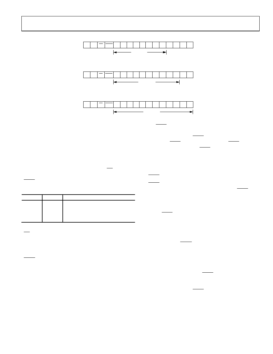
BIT15
(MSB)
A1
A0
D7
D6 D5 D4 D3
D2
D1
D0
0
X
BIT0
(LSB)
PD LDAC
DATA BITS
0
09
29
-03
2
Figure 32. AD5304 Input Shift Register Contents
BIT15
(MSB)
BIT0
(LSB)
A1
A0
D7
D8
D9
D6
D5 D4
D3
D2
D1
D0
X
PD LDAC
DATA BITS
00
92
9-
03
3
Figure 33. AD5314 Input Shift Register Contents
BIT15
(MSB)
BIT0
(LSB)
A1
A0
D7
D8
D9
D10
D11
D6
D5 D4
D3
D2
D1
D0
PD LDAC
DATA BITS
00
92
9-
0
34
Figure 34. AD5324 Input Shift Register Contents
Input Shift Register
The input shift register is 16 bits wide. Data is loaded into the
device as a 16-bit word under the control of a serial clock input,
SCLK. See Figure 2 for the timing diagram of this operation. The
16-bit word consists of four control bits followed by 8, 10, or 12
bits of DAC data, depending on the device type. Data is loaded
MSB first (Bit 15) and the first two bits determine whether the
data is for DAC A, DAC B, DAC C, or DAC D. Bit 13 and Bit 12
control the operating mode of the DAC. Bit 13 is PD, and deter-
mines whether the part is in normal or power-down mode. Bit 12 is
LDAC, and controls when DAC registers and outputs are updated.
Table 6. Address Bits
A1
A0
DAC Addressed
0
DAC A
0
1
DAC B
1
0
DAC C
1
DAC D
Address and Control Bits
PD
0: All four DACs go into power-down mode, consuming
only 200 nA @ 5 V. The DAC outputs enter a high
impedance state.
1: Normal operation.
LDAC
0: All four DAC registers and, therefore, all DAC outputs
updated simultaneously on completion of the write
sequence.
1: Only addressed input register is updated. There is
no change in the content of the DAC registers.
The AD5324 uses all 12 bits of DAC data; the AD5314 uses 10 bits
and ignores the 2 LSB Bits. The AD5304 uses eight bits and ignores
the last four bits. The data format is straight binary, with all 0s
corresponding to 0 V output and all 1s corresponding to full-scale
output (VREF 1 LSB).
The SYNC input is a level-triggered input that acts as a frame
synchronization signal and chip enable. Data can be transferred
into the device only while SYNC is low. To start the serial data
transfer, take SYNC low, observing the minimum SYNC to SCLK
falling edge setup time, t4. After SYNC goes low, serial data shifts
into the device’s input shift register on the falling edges of SCLK
for 16 clock pulses. Any data and clock pulses after the 16th falling
edge of SCLK are ignored because the SCLK and DIN input buffers
are powered down. No further serial data transfer occurs until
SYNC is taken high and low again.
SYNC can be taken high after the falling edge of the 16th SCLK
pulse, observing the minimum SCLK falling edge to SYNC
rising edge time, t7.
After the end of the serial data transfer, data automatically transfers
from the input shift register to the input register of the selected
DAC. If SYNC is taken high before the 16th falling edge of SCLK,
the data transfer is aborted and the DAC input registers are not
updated.
When data has been transferred into three of the DAC input
registers, all DAC registers and all DAC outputs are simultaneously
updated by setting LDAC low when writing to the remaining
DAC input register.
Low Power Serial Interface
To reduce the power consumption of the device even further, the
interface fully powers up only when the device is being written
to, that is, on the falling edge of SYNC. As soon as the 16-bit
control word has been written to the part, the SCLK and DIN
input buffers are powered down. They power up again only
following a falling edge of SYNC.
相关PDF资料 |
PDF描述 |
|---|---|
| NB6L11DTR2G | IC CLK BUFFER TRANSLA 1:2 8TSSOP |
| VE-J5K-MY | CONVERTER MOD DC/DC 40V 50W |
| NB6L11DR2G | IC CLK BUFFER TRANSLA 1:2 8-SOIC |
| VE-J54-MY | CONVERTER MOD DC/DC 48V 50W |
| V48A48H500BF2 | CONVERTER MOD DC/DC 48V 500W |
相关代理商/技术参数 |
参数描述 |
|---|---|
| AD5314BRMZ | 功能描述:IC DAC 10BIT QUAD VOUT 10-MSOP RoHS:是 类别:集成电路 (IC) >> 数据采集 - 数模转换器 系列:- 产品培训模块:Lead (SnPb) Finish for COTS Obsolescence Mitigation Program 标准包装:50 系列:- 设置时间:4µs 位数:12 数据接口:串行 转换器数目:2 电压电源:单电源 功率耗散(最大):- 工作温度:-40°C ~ 85°C 安装类型:表面贴装 封装/外壳:8-TSSOP,8-MSOP(0.118",3.00mm 宽) 供应商设备封装:8-uMAX 包装:管件 输出数目和类型:2 电压,单极 采样率(每秒):* 产品目录页面:1398 (CN2011-ZH PDF) |
| AD5314BRMZ-REEL | 功能描述:IC DAC 10BIT QUAD VOUT 10MSOP TR RoHS:是 类别:集成电路 (IC) >> 数据采集 - 数模转换器 系列:- 产品培训模块:LTC263x 12-, 10-, and 8-Bit VOUT DAC Family 特色产品:LTC2636 - Octal 12-/10-/8-Bit SPI VOUT DACs with 10ppm/°C Reference 标准包装:91 系列:- 设置时间:4µs 位数:10 数据接口:MICROWIRE?,串行,SPI? 转换器数目:8 电压电源:单电源 功率耗散(最大):2.7mW 工作温度:-40°C ~ 85°C 安装类型:表面贴装 封装/外壳:14-WFDFN 裸露焊盘 供应商设备封装:14-DFN-EP(4x3) 包装:管件 输出数目和类型:8 电压,单极 采样率(每秒):* |
| AD5314BRMZ-REEL7 | 功能描述:IC DAC 10BIT QUAD VOUT 10MSOP TR RoHS:是 类别:集成电路 (IC) >> 数据采集 - 数模转换器 系列:- 产品培训模块:LTC263x 12-, 10-, and 8-Bit VOUT DAC Family 特色产品:LTC2636 - Octal 12-/10-/8-Bit SPI VOUT DACs with 10ppm/°C Reference 标准包装:91 系列:- 设置时间:4µs 位数:10 数据接口:MICROWIRE?,串行,SPI? 转换器数目:8 电压电源:单电源 功率耗散(最大):2.7mW 工作温度:-40°C ~ 85°C 安装类型:表面贴装 封装/外壳:14-WFDFN 裸露焊盘 供应商设备封装:14-DFN-EP(4x3) 包装:管件 输出数目和类型:8 电压,单极 采样率(每秒):* |
| AD5314WARMZ-REEL7 | 制造商:Analog Devices 功能描述:DAC 4-CH Resistor-String 10-bit 10-Pin MSOP T/R 制造商:Analog Devices 功能描述:10-BIT QUAD DAC I.C. - Tape and Reel |
| AD5315 | 制造商:AD 制造商全称:Analog Devices 功能描述:2.5 V to 5.5 V, 500 uA, Parallel Interface Quad Voltage-Output 8-/10-/12-Bit DACs |
发布紧急采购,3分钟左右您将得到回复。