参数资料
| 型号: | AD5316BRUZ |
| 厂商: | Analog Devices Inc |
| 文件页数: | 15/24页 |
| 文件大小: | 0K |
| 描述: | IC DAC 10BIT QUAD W/BUFF 16TSSOP |
| 产品培训模块: | Data Converter Fundamentals DAC Architectures |
| 标准包装: | 96 |
| 设置时间: | 7µs |
| 位数: | 10 |
| 数据接口: | I²C,串行 |
| 转换器数目: | 4 |
| 电压电源: | 单电源 |
| 功率耗散(最大): | 4.5mW |
| 工作温度: | -40°C ~ 105°C |
| 安装类型: | 表面贴装 |
| 封装/外壳: | 16-TSSOP(0.173",4.40mm 宽) |
| 供应商设备封装: | 16-TSSOP |
| 包装: | 管件 |
| 输出数目和类型: | 4 电压,单极;4 电压,双极 |
| 采样率(每秒): | 143k |
| 产品目录页面: | 782 (CN2011-ZH PDF) |
AD5306/AD5316/AD5326
Rev. F | Page 22 of 24
POWER SUPPLY DECOUPLING
In any circuit where accuracy is important, careful consideration
of the power supply and ground return layout helps to ensure
the rated performance. The printed circuit board on which the
AD5306/AD5316/AD5326 is mounted should be designed so
the analog and digital sections are separated and confined to
certain areas of the board.
If the AD5306/AD5316/AD5326 is in a system where multiple
devices require an AGND-to-DGND connection, the connection
should be made at one point only. The star ground point should
be established as close as possible to the device. The AD5306/
AD5316/AD5326 should have ample supply bypassing of 10 μF
in parallel with 0.1 μF on the supply located as close to the
package as possible, ideally right up against the device. The 10 μF
capacitors are the tantalum bead type. The 0.1 μF capacitor should
have low effective series resistance (ESR) and low effective
series inductance (ESI), like the common ceramic types that
provide a low impedance path to ground at high frequencies to
handle transient currents due to internal logic switching.
The power supply lines of the AD5306/AD5316/AD5326 should
use as large a trace as possible to provide low impedance paths
and reduce the effects of glitches on the power supply line.
Components with fast-switching signals, such as clocks, should
be shielded with digital ground to avoid radiating noise to other
parts of the board, and they should never be run near the
reference inputs. A ground line routed between the SDA and
SCL lines helps to reduce crosstalk between them. Although a
ground line is not required on a multilayer board because there is
a separate ground plane, separating the lines helps.
Avoid crossover of digital and analog signals. Traces on opposite
sides of the board should run at right angles to each other. This
reduces the effects of feedthrough through the board. A micro-
strip technique is the best method, but its use is not always
possible with a double-sided board. In this technique, the
component side of the board is dedicated to ground plane while
signal traces are placed on the solder side.
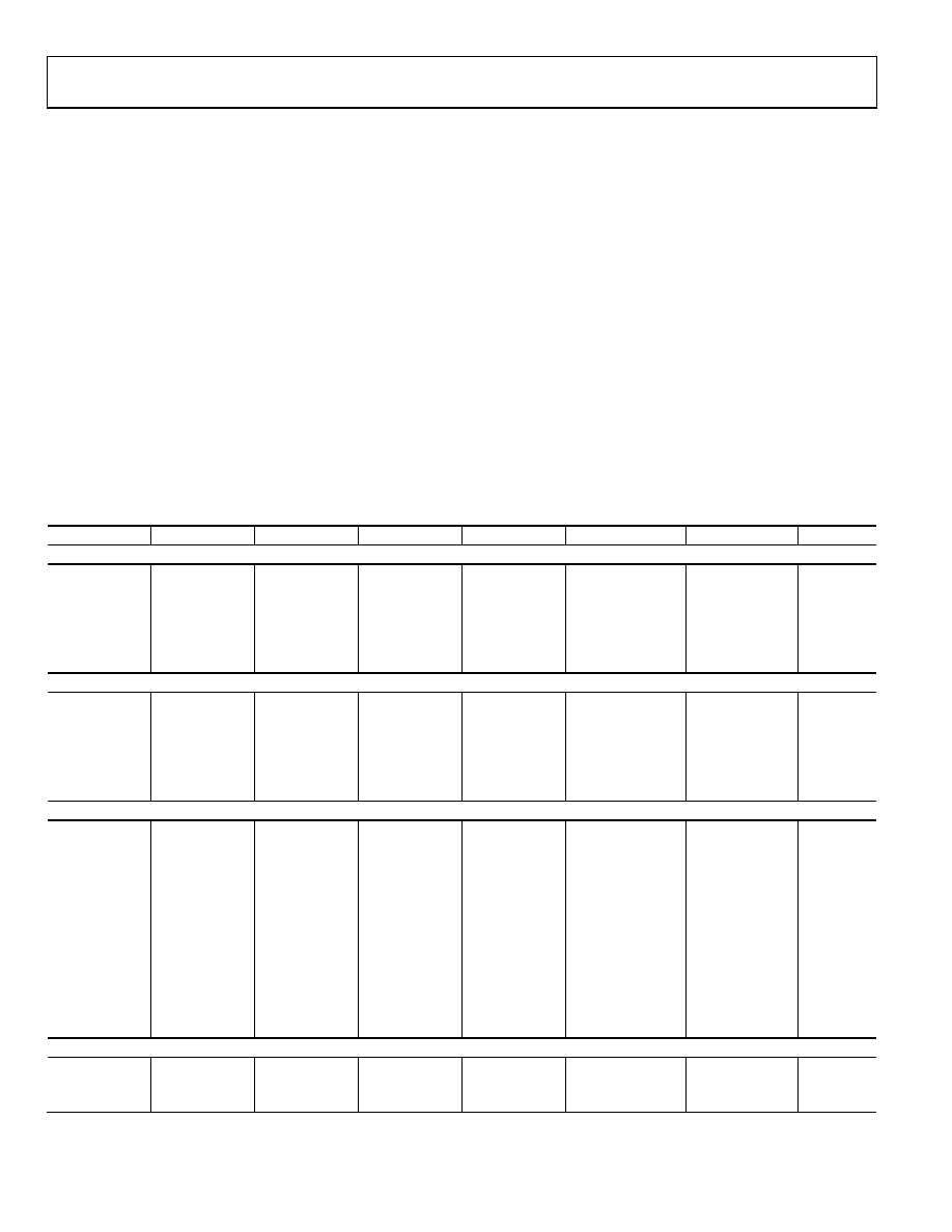
Table 8. Overview of AD53xx Serial Devices1
Part No.
Resolution
No. of DACs
DNL
Interface
Settling Time (μs)
Package
Pins
SINGLES
AD5300
8
1
±0.25
SPI
4
SOT-23, MSOP
6, 8
AD5310
10
1
±0.5
SPI
6
SOT-23, MSOP
6, 8
AD5320
12
1
±1.0
SPI
8
SOT-23, MSOP
6, 8
AD5301
8
1
±0.25
2-wire
6
SOT-23, MSOP
6, 8
AD5311
10
1
±0.5
2-wire
7
SOT-23, MSOP
6, 8
AD5321
12
1
±1.0
2-wire
8
SOT-23, MSOP
6, 8
DUALS
AD5302
8
2
±0.25
SPI
6
MSOP
8
AD5312
10
2
±0.5
SPI
7
MSOP
8
AD5322
12
2
±1.0
SPI
8
MSOP
8
AD5303
8
2
±0.25
SPI
6
TSSOP
16
AD5313
10
2
±0.5
SPI
7
TSSOP
16
AD5323
12
2
±1.0
SPI
8
TSSOP
16
QUADS
AD5304
8
4
±0.25
SPI
6
MSOP
10
AD5314
10
4
±0.5
SPI
7
MSOP
10
AD5324
12
4
±1.0
SPI
8
MSOP
10
AD5305
8
4
±0.25
2-Wire
6
MSOP
10
AD5315
10
4
±0.5
2-Wire
7
MSOP
10
AD5325
12
4
±1.0
2-Wire
8
MSOP
10
AD5306
8
4
±0.25
2-Wire
6
TSSOP
16
AD5316
10
4
±0.5
2-Wire
7
TSSOP
16
AD5326
12
4
±1.0
2-Wire
8
TSSOP
16
AD5307
8
4
±0.25
SPI
6
TSSOP
16
AD5317
10
4
±0.5
SPI
7
TSSOP
16
AD5327
12
4
±1.0
SPI
8
TSSOP
16
OCTALS
AD5308
8
±0.25
SPI
6
TSSOP
16
AD5318
10
8
±0.5
SPI
7
TSSOP
16
AD5328
12
8
±1.0
SPI
8
TSSOP
16
1 Visit www.analog.com/support/standard_linear/selection_guides/AD53xx.html for more information.
相关PDF资料 |
PDF描述 |
|---|---|
| ICS843001CGILFT | IC CLK GEN FIBRE CH 8TSSOP |
| VI-2NX-MW-F1 | CONVERTER MOD DC/DC 5.2V 100W |
| VE-J53-MZ-F3 | CONVERTER MOD DC/DC 24V 25W |
| VI-2TT-MY-F1 | CONVERTER MOD DC/DC 6.5V 50W |
| VE-J4K-MZ-F1 | CONVERTER MOD DC/DC 40V 25W |
相关代理商/技术参数 |
参数描述 |
|---|---|
| AD5316BRUZ1 | 制造商:AD 制造商全称:Analog Devices 功能描述:2.5 V to 5.5 V, 400 ??A, 2-Wire Interface, Quad Voltage Output, 8-/10-/12-Bit DACs |
| AD5316BRUZ-REEL | 功能描述:IC DAC 10BIT QUAD W/BUFF 16TSSOP RoHS:是 类别:集成电路 (IC) >> 数据采集 - 数模转换器 系列:- 标准包装:2,400 系列:- 设置时间:- 位数:18 数据接口:串行 转换器数目:3 电压电源:模拟和数字 功率耗散(最大):- 工作温度:-40°C ~ 85°C 安装类型:表面贴装 封装/外壳:36-TFBGA 供应商设备封装:36-TFBGA 包装:带卷 (TR) 输出数目和类型:* 采样率(每秒):* |
| AD5316BRUZ-REEL1 | 制造商:AD 制造商全称:Analog Devices 功能描述:2.5 V to 5.5 V, 400 ??A, 2-Wire Interface, Quad Voltage Output, 8-/10-/12-Bit DACs |
| AD5316BRUZ-REEL7 | 功能描述:IC DAC 10BIT QUAD W/BUFF 16TSSOP RoHS:是 类别:集成电路 (IC) >> 数据采集 - 数模转换器 系列:- 产品培训模块:LTC263x 12-, 10-, and 8-Bit VOUT DAC Family 特色产品:LTC2636 - Octal 12-/10-/8-Bit SPI VOUT DACs with 10ppm/°C Reference 标准包装:91 系列:- 设置时间:4µs 位数:10 数据接口:MICROWIRE?,串行,SPI? 转换器数目:8 电压电源:单电源 功率耗散(最大):2.7mW 工作温度:-40°C ~ 85°C 安装类型:表面贴装 封装/外壳:14-WFDFN 裸露焊盘 供应商设备封装:14-DFN-EP(4x3) 包装:管件 输出数目和类型:8 电压,单极 采样率(每秒):* |
| AD5316BRUZ-REEL71 | 制造商:AD 制造商全称:Analog Devices 功能描述:2.5 V to 5.5 V, 400 ??A, 2-Wire Interface, Quad Voltage Output, 8-/10-/12-Bit DACs |
发布紧急采购,3分钟左右您将得到回复。