参数资料
| 型号: | AD5322BRM |
| 厂商: | Analog Devices Inc |
| 文件页数: | 7/24页 |
| 文件大小: | 0K |
| 描述: | IC DAC 12BIT DUAL R-R OUT 10MSOP |
| 产品培训模块: | Data Converter Fundamentals DAC Architectures |
| 标准包装: | 50 |
| 设置时间: | 6µs |
| 位数: | 12 |
| 数据接口: | 串行 |
| 转换器数目: | 2 |
| 电压电源: | 单电源 |
| 功率耗散(最大): | 2.5mW |
| 工作温度: | -40°C ~ 105°C |
| 安装类型: | 表面贴装 |
| 封装/外壳: | 10-TFSOP,10-MSOP(0.118",3.00mm 宽) |
| 供应商设备封装: | 10-MSOP |
| 包装: | 管件 |
| 输出数目和类型: | 2 电压,单极;2 电压,双极 |
| 采样率(每秒): | 125k |
AD5302/AD5312/AD5322
Rev. D | Page 15 of 24
SERIAL INTERFACE
The AD5302/AD5312/AD5322 are controlled over a versatile,
3-wire serial interface, which operates at clock rates up to 30 MHz
and is compatible with SPI, QSPI, MICROWIRE, and DSP
interface standards.
INPUT SHIFT REGISTER
Data is loaded into the device as a 16-bit word under the control
of a serial clock input, SCLK. The timing diagram for this
operation is shown in Figure 2. The 16-bit word consists of four
control bits followed by 8, 10, or 12 bits of DAC data, depending
on the device type. The first bit loaded is the MSB (Bit 15),
which determines whether the data is for DAC A or DAC B.
Bit 14 determines if the reference input is buffered or unbuffered.
Bit 13 and Bit 12 control the operating mode of the DAC.
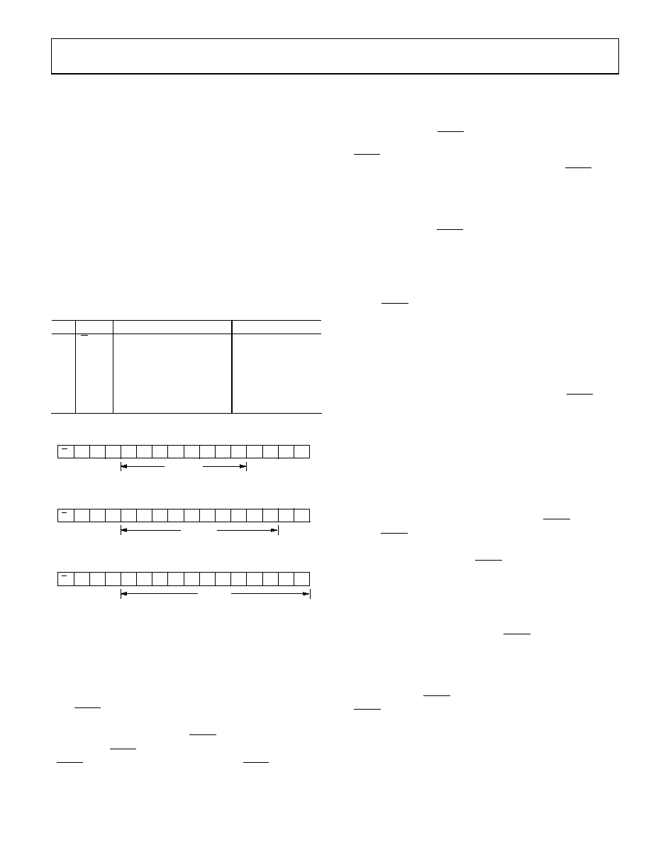
Table 6. Control Bits
Bit
Name
Function
Power-On Default
15
A/B
0: Data Written to DAC A
N/A
1: Data Written to DAC B
14
BUF
0: Reference Is Unbuffered
0
1: Reference Is Buffered
13
PD1
Mode Bit
0
12
PD0
Mode Bit
0
BIT 15
(MSB)
BIT 0
(LSB)
PD0
D7D6
D5D4D3D2D1
D0
PD1
BUF
XX
DATA BITS
00928-
030
A/B
Figure 30. AD5302 Input Shift Register Contents
BIT 15
(MSB)
BIT 0
(LSB)
PD0
D7D6D5D4D3D2D1D0
PD1
BUF
XX
DATA BITS
00928-
031
A/B
D9
D8
Figure 31. AD5312 Input Shift Register Contents
BIT 15
(MSB)
BIT 0
(LSB)
PD0
D7D6D5D4
D3D2D1D0
PD1
BUF
DATA BITS
00928-
032
A/B
D9
D8
D11 D10
Figure 32. AD5322 Input Shift Register Contents
The remaining bits are DAC data bits, starting with the MSB and
ending with the LSB. The AD5322 uses all 12 bits of DAC data,
the AD5312 uses 10 bits and ignores the 2 LSB. The AD5302 uses
eight bits and ignores the last four bits. The data format is straight
binary, with all 0s corresponding to 0 V output, and all 1s
corresponding to full-scale output (VREF – 1 LSB).
The SYNC input is a level-triggered input that acts as a frame
synchronization signal and chip enable. Data can only be
transferred into the device while SYNC is low. To start the serial
data transfer, SYNC should be taken low observing the minimum
SYNC to SCLK active edge setup time, t4. After SYNC goes low,
serial data is shifted into the device’s input shift register on the
falling edges of SCLK for 16 clock pulses. Any data and clock
pulses after the 16th are ignored, and no further serial data
transfers occur until SYNC is taken high and low again.
SYNC can be taken high after the falling edge of the 16th SCLK
pulse, observing the minimum SCLK falling edge to SYNC
rising edge time, t7.
After the end of serial data transfer, data is automatically
transferred from the input shift register to the input register of
the selected DAC. If SYNC is taken high before the 16th falling
edge of SCLK, the data transfer is aborted and the input
registers are not updated.
When data has been transferred into both input registers, the
DAC registers of both DACs can be simultaneously updated by
taking LDAC low.
LOW POWER SERIAL INTERFACE
To reduce the power consumption of the device even further,
the interface only powers up fully when the device is being
written to. As soon as the 16-bit control word has been written
to the part, the SCLK and DIN input buffers are powered down.
They only power up again following a falling edge of SYNC.
DOUBLE-BUFFERED INTERFACE
The AD5302/AD5312/AD5322 DACs all have double-buffered
interfaces consisting of two banks of registers—input registers and
DAC registers. The input register is connected directly to the input
shift register and the digital code is transferred to the relevant input
register on completion of a valid write sequence. The DAC
register contains the digital code used by the resistor string.
Access to the DAC register is controlled by the LDAC function.
When LDAC is high, the DAC register is latched and the input
register can change state without affecting the contents of the
DAC register. However, when LDAC is brought low, the DAC
register becomes transparent and the contents of the input
register are transferred to it.
This is useful if the user requires simultaneous updating of both
DAC outputs. The user can write to both input registers
individually and then, by pulsing the LDAC input low, both
outputs update simultaneously.
These parts contain an extra feature whereby the DAC register
is not updated unless its input register has been updated since
the last time that LDAC was brought low. Normally, when
LDAC is brought low, the DAC registers are filled with the
contents of the input registers. In the case of the AD5302/
AD5312/AD5322, the part only updates the DAC register if
the input register has been changed since the last time the
DAC register was updated, thereby removing unnecessary
digital crosstalk.
相关PDF资料 |
PDF描述 |
|---|---|
| AD5323BRU | IC DAC 12 BIT DUAL R-R 16-TSSOP |
| AD5324BRM | IC DAC 12BIT QUAD 2.5V 10-MSOP |
| AD5325ARM | IC DAC 12BIT 2WIRE I2C 10-MSOP |
| AD5326BRU | IC DAC 12BIT QUAD W/BUFF 16TSSOP |
| AD5327BRU | IC DAC 12BIT QUAD 2.5V 16-TSSOP |
相关代理商/技术参数 |
参数描述 |
|---|---|
| AD5322BRM-REEL | 制造商:Analog Devices 功能描述:DAC 2-CH Resistor-String 12-bit 10-Pin MSOP T/R 制造商:Analog Devices 功能描述:DAC 2CH RES-STRING 12-BIT 10MSOP - Tape and Reel |
| AD5322BRM-REEL7 | 功能描述:IC DAC 12BIT DUAL W/BUFF 10-MSOP RoHS:否 类别:集成电路 (IC) >> 数据采集 - 数模转换器 系列:- 标准包装:47 系列:- 设置时间:2µs 位数:14 数据接口:并联 转换器数目:1 电压电源:单电源 功率耗散(最大):55µW 工作温度:-40°C ~ 85°C 安装类型:表面贴装 封装/外壳:28-SSOP(0.209",5.30mm 宽) 供应商设备封装:28-SSOP 包装:管件 输出数目和类型:1 电流,单极;1 电流,双极 采样率(每秒):* |
| AD5322BRMZ | 功能描述:IC DAC 12BIT DUAL 10MSOP RoHS:是 类别:集成电路 (IC) >> 数据采集 - 数模转换器 系列:- 产品培训模块:Lead (SnPb) Finish for COTS Obsolescence Mitigation Program 标准包装:50 系列:- 设置时间:4µs 位数:12 数据接口:串行 转换器数目:2 电压电源:单电源 功率耗散(最大):- 工作温度:-40°C ~ 85°C 安装类型:表面贴装 封装/外壳:8-TSSOP,8-MSOP(0.118",3.00mm 宽) 供应商设备封装:8-uMAX 包装:管件 输出数目和类型:2 电压,单极 采样率(每秒):* 产品目录页面:1398 (CN2011-ZH PDF) |
| AD5322BRMZ-REEL | 功能描述:IC DAC 12BIT DUAL 10MSOP T/R RoHS:是 类别:集成电路 (IC) >> 数据采集 - 数模转换器 系列:- 产品培训模块:LTC263x 12-, 10-, and 8-Bit VOUT DAC Family 特色产品:LTC2636 - Octal 12-/10-/8-Bit SPI VOUT DACs with 10ppm/°C Reference 标准包装:91 系列:- 设置时间:4µs 位数:10 数据接口:MICROWIRE?,串行,SPI? 转换器数目:8 电压电源:单电源 功率耗散(最大):2.7mW 工作温度:-40°C ~ 85°C 安装类型:表面贴装 封装/外壳:14-WFDFN 裸露焊盘 供应商设备封装:14-DFN-EP(4x3) 包装:管件 输出数目和类型:8 电压,单极 采样率(每秒):* |
| AD5322BRMZ-REEL7 | 功能描述:IC DAC 12BIT DUAL 10MSOP T/R RoHS:是 类别:集成电路 (IC) >> 数据采集 - 数模转换器 系列:- 产品培训模块:LTC263x 12-, 10-, and 8-Bit VOUT DAC Family 特色产品:LTC2636 - Octal 12-/10-/8-Bit SPI VOUT DACs with 10ppm/°C Reference 标准包装:91 系列:- 设置时间:4µs 位数:10 数据接口:MICROWIRE?,串行,SPI? 转换器数目:8 电压电源:单电源 功率耗散(最大):2.7mW 工作温度:-40°C ~ 85°C 安装类型:表面贴装 封装/外壳:14-WFDFN 裸露焊盘 供应商设备封装:14-DFN-EP(4x3) 包装:管件 输出数目和类型:8 电压,单极 采样率(每秒):* |
发布紧急采购,3分钟左右您将得到回复。