参数资料
| 型号: | AD5323ARUZ |
| 厂商: | Analog Devices Inc |
| 文件页数: | 14/28页 |
| 文件大小: | 0K |
| 描述: | IC DAC 12BIT DUAL R-R 16-TSSOP |
| 产品培训模块: | Data Converter Fundamentals DAC Architectures |
| 标准包装: | 96 |
| 设置时间: | 8µs |
| 位数: | 12 |
| 数据接口: | 串行 |
| 转换器数目: | 2 |
| 电压电源: | 单电源 |
| 功率耗散(最大): | 2.5mW |
| 工作温度: | -40°C ~ 105°C |
| 安装类型: | 表面贴装 |
| 封装/外壳: | 16-TSSOP(0.173",4.40mm 宽) |
| 供应商设备封装: | 16-TSSOP |
| 包装: | 管件 |
| 输出数目和类型: | 2 电压,单极;2 电压,双极 |
| 采样率(每秒): | 125k |
第1页第2页第3页第4页第5页第6页第7页第8页第9页第10页第11页第12页第13页当前第14页第15页第16页第17页第18页第19页第20页第21页第22页第23页第24页第25页第26页第27页第28页
AD5303/AD5313/AD5323
Rev. B | Page 21 of 28
APPLICATIONS INFORMATION
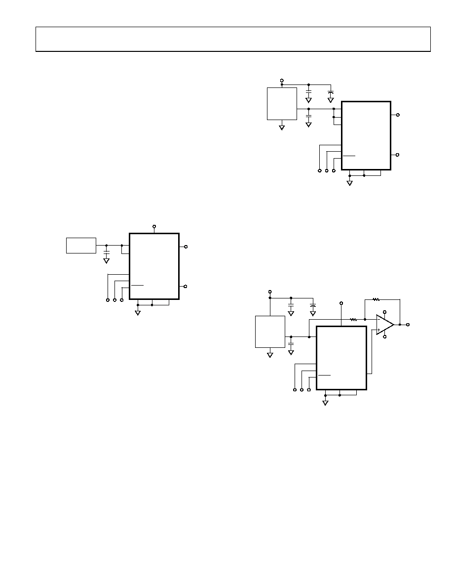
TYPICAL APPLICATION CIRCUIT
The AD5303/AD5313/AD5323 can be used with a wide range
of reference voltages, especially if the reference inputs are con-
figured to be unbuffered, in which case the devices offer a full,
one-quadrant multiplying capability over a reference range of
0 V to VDD.
More typically, the AD5303/AD5313/AD5323 may be used
with a fixed precision reference voltage. Figure 39 shows a
typical setup for the AD5303/AD5313/AD5323 when using
an external reference. If the reference inputs are unbuffered,
the reference input range is from 0 V to VDD, but if the on-chip
reference buffers are used, the reference range is reduced. Suit-
(2.5 V references). For 2.5 V operation, a suitable external
reference is the REF191, a 2.048 V reference.
SCLK
DIN
GND
AD5303/AD5313/
AD5323
SERIAL
INTERFACE
EXT
REF
00
47
2-
03
9
AD780/REF192
WITH VDD = 5V
OR REF191 WITH
VDD = 2.5V
VOUT
SYNC
VOUTA
VOUTB
VREFA
VREFB
1F
VDD = 2.5V to 5.5V
VDD
BUF A BUF B
Figure 39. AD5303/AD5313/AD5323 Using External Reference
If an output range of 0 V to VDD is required when the reference
inputs are configured as unbuffered (for example, 0 V to 5 V),
the simplest solution is to connect the reference inputs to VDD.
As this supply may not be very accurate and may be noisy, the
AD5303/AD5313/AD5323 can be powered from the reference
voltage, for example, using a 5 V reference such as the REF195,
voltage for the AD5303/AD5313/AD5323. The supply current
required from the REF195 is 300 μA and approximately 30 μA
or 60 μA into each of the reference inputs (if unbuffered). This
is with no load on the DAC outputs. When the DAC outputs are
loaded, the REF195 also needs to supply the current to the
loads. The total current required (with a 10 kΩ load on each
output) is
360 μA + 2(5 V/10 kΩ) = 1.36 mA
The load regulation of the REF195 is typically 2 ppm/mA, which
results in an error of 2.7 ppm (13.5 μV) for the 1.36 mA current
drawn from it. This corresponds to a 0.0007 LSB error at eight
bits and 0.011 LSB error at 12 bits.
SCLK
DIN
AD5303/AD5313/
AD5323
SERIAL
INTERFACE
REF195
00
47
2-
0
40
OUTPUT
SYNC
VOUTA
VOUTB
VDD
VREFA
1F
15V
GND
VS
VREFB
0.1F
10F
GND BUF A BUF B
Figure 40. Using an REF195 as Power and Reference to the
AD5303/AD5313/AD5323
BIPOLAR OPERATION USING THE AD5303/
AD5313/AD5323
The AD5303/AD5313/AD5323 have been designed for single-
supply operation, but bipolar operation is also achievable using
the circuit shown in Figure 41. The circuit shown has been con-
figured to achieve an output voltage range of 5 V < VOUT < +5 V.
Rail-to-rail operation at the amplifier output is achievable using
SCLK
DIN
AD5303/AD5313/
AD5323
SERIAL
INTERFACE
REF195
00
47
2-
04
1
SYNC
VOUTA/B
VREFA/B
1F
GND
6V to 16V
0.1F
10F
VDD
VDD = 5V
+5V
–5V
R2
10k
AD820/
OP295
R1
10k
±5V
GND BUF A BUF B
OUTPUT
VS
Figure 41. Bipolar Operation Using the AD5303/AD5313/AD5323
The output voltage for any input code can be calculated as
follows:
[
])
/
(
/
)
(
)
2
/
(
)
(
R1
R2
V
R1
R2
R1
D
V
REF
N
REF
OUT
×
+
×
=
where:
D is the decimal equivalent of the code loaded to the DAC.
N is the DAC resolution.
VREF is the reference voltage input, and gain bit = 0, with
VREF = 5 V
R1 = R2 = 10 kΩ and VDD = 5 V,
V
D
V
N
OUT
5
)
2
/
10
(
×
=
相关PDF资料 |
PDF描述 |
|---|---|
| LTC2624CGN-1#TRPBF | IC DAC 12BIT QUAD R-R OUT 16SSOP |
| V150A12H500BL3 | CONVERTER MOD DC/DC 12V 500W |
| SY10E111AJC TR | IC CLK FANOUT BUFFER 1:9 28-PLCC |
| LTC2629CGN-1#TRPBF | IC DAC 12BIT R-R QUAD 16SSOP |
| V150A12H500BG | CONVERTER MOD DC/DC 12V 500W |
相关代理商/技术参数 |
参数描述 |
|---|---|
| AD5323ARUZ1 | 制造商:AD 制造商全称:Analog Devices 功能描述:2.5 V to 5.5 V, 230 ??A, Dual Rail-to-Rail Voltage Output 8-/10-/12-Bit DACs |
| AD5323ARUZ-REEL7 | 功能描述:IC DAC 12BIT DUAL R-R 16-TSSOP RoHS:是 类别:集成电路 (IC) >> 数据采集 - 数模转换器 系列:- 标准包装:2,400 系列:- 设置时间:- 位数:18 数据接口:串行 转换器数目:3 电压电源:模拟和数字 功率耗散(最大):- 工作温度:-40°C ~ 85°C 安装类型:表面贴装 封装/外壳:36-TFBGA 供应商设备封装:36-TFBGA 包装:带卷 (TR) 输出数目和类型:* 采样率(每秒):* |
| AD5323ARUZ-REEL71 | 制造商:AD 制造商全称:Analog Devices 功能描述:2.5 V to 5.5 V, 230 ??A, Dual Rail-to-Rail Voltage Output 8-/10-/12-Bit DACs |
| AD5323BRU | 功能描述:IC DAC 12 BIT DUAL R-R 16-TSSOP RoHS:否 类别:集成电路 (IC) >> 数据采集 - 数模转换器 系列:- 标准包装:47 系列:- 设置时间:2µs 位数:14 数据接口:并联 转换器数目:1 电压电源:单电源 功率耗散(最大):55µW 工作温度:-40°C ~ 85°C 安装类型:表面贴装 封装/外壳:28-SSOP(0.209",5.30mm 宽) 供应商设备封装:28-SSOP 包装:管件 输出数目和类型:1 电流,单极;1 电流,双极 采样率(每秒):* |
| AD5323BRU-REEL | 制造商:Analog Devices 功能描述:DAC 2-CH Resistor-String 12-bit 16-Pin TSSOP T/R 制造商:Analog Devices 功能描述:DAC 2CH RES-STRING 12-BIT 16TSSOP - Tape and Reel |
发布紧急采购,3分钟左右您将得到回复。